Page 48 - ChipScale_May-June_2020-digital
P. 48
is for an essential part limited by the
                                                                             interconnect. Therefore, building more
                                                                             compact logic circuits by track height
                                                                             scaling would require an optimization of
                                                                             the routability at the block level to enable
                                                                             the introduction of these new device
                                                                             architectures at reduced track heights.
                                                                             For example, as explained above, the
                                                                             transition from 6T to 5T standard cell
                                                                             height can only be enabled by moving the
                                                                             power rails – traditionally implemented in
                                                                             the chip’s BEOL (i.e., M int  and M1 layers)
                                                                             – to the FEOL.
                                                                               In the forksheet architecture, the local
                                                                             interconnect (active trench contact) to
                                                                             connect p- and nMOS source/drain within
                                                                             the same vertical trench can be more
                                                                             efficiently used in standard cell routing.
                                                                             This n-to-p-routing results in reduced M1
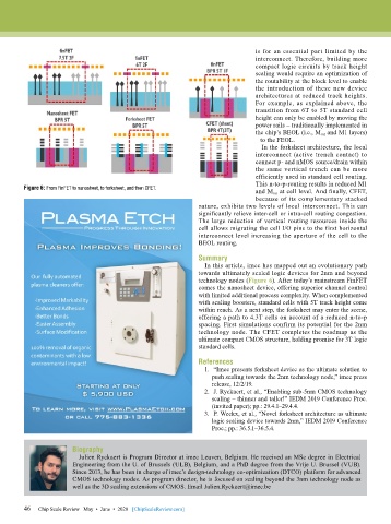
        Figure 6: From FinFET to nanosheet, to forksheet, and then CFET.
                                                                             and M int  at cell level. And finally, CFET,
                                                                             because of its complementary stacked
                                                            nature, exhibits two levels of local interconnect. This can
                                                            significantly relieve inter-cell or intra-cell routing congestion.
                                                            The large reduction of vertical routing resources inside the
                                                            cell allows migrating the cell I/O pins to the first horizontal
                                                            interconnect level increasing the aperture of the cell to the
                                                            BEOL routing.

                                                            Summary
                                                              In this article, imec has mapped out an evolutionary path
                                                            towards ultimately scaled logic devices for 2nm and beyond
                                                            technology nodes (Figure 6). After today’s mainstream FinFET
                                                            comes the nanosheet device, offering superior channel control
                                                            with limited additional process complexity. When complemented
                                                            with scaling boosters, standard cells with 5T track height come
                                                            within reach. As a next step, the forksheet may enter the scene,
                                                            offering a path to 4.3T cells on account of a reduced n-to-p
                                                            spacing. First simulations confirm its potential for the 2nm
                                                            technology node. The CFET completes the roadmap as the
                                                            ultimate compact CMOS structure, holding promise for 3T logic
                                                            standard cells.

                                                            References
                                                              1.  “Imec presents forksheet device as the ultimate solution to
                                                                push scaling towards the 2nm technology node,” imec press
                                                                release, 12/2/19.
                                                              2.  J. Ryckaert, et al., “Enabling sub-5nm CMOS technology
                                                                scaling – thinner and taller!” IEDM 2019 Conference Proc.
                                                                (invited paper); pp.: 29.4.1–29.4.4.
                                                              3.  P. Weckx, et al., “Novel forksheet architecture as ultimate
                                                                logic scaling device towards 2nm,” IEDM 2019 Conference
                                                                Proc.; pp.: 36.5.1–36.5.4.


                       Biography
                         Julien Ryckaert is Program Director at imec Leuven, Belgium. He received an MSc degree in Electrical
                       Engineering from the U. of Brussels (ULB), Belgium, and a PhD degree from the Vrije U. Brussel (VUB).
                       Since 2013, he has been in charge of imec’s design-technology co-optimization (DTCO) platform for advanced
                       CMOS technology nodes. As program director, he is focused on scaling beyond the 3nm technology node as
                       well as the 3D scaling extensions of CMOS. Email Julien.Ryckaert@imec.be


        46   Chip Scale Review   May  •  June  •  2020   [ChipScaleReview.com]
        46

