Page 40 - ChipScale_May-June_2020-digital
P. 40
Demand for 3D devices drives inspection


                           and metrology innovation


                           CSR asked Raj Jammy, President of the Process Control Solutions Business Unit at Carl Zeiss SMT
                           group and President of Carl Zeiss SMT Inc., the North America subsidiary of Carl Zeiss SMT GmbH,
                           to provide an update on how demand for 3D devices is driving inspection and metrology innovation.


          CSR: 3D devices drive a good deal   scanning electron microscopy (SEM)   RJ: Generally, advanced packages are
        of semiconductor technologies today   imaging to FIB prep and TEM imaging,   used for the advanced Si nodes that use
        and in turn, such devices need to have   today we see the cycle repeat with package   fragile dielectric materials in the back end
        3D integrated information when it   fine pitches driving a transition from   of line (BEOL) Si interconnects. To achieve
        comes to 3D inspection and metrology.   traditional cross-sectional methods to new   fine pitches, Cu-pillar solder bumps are
        Why is imaging alone not sufficient for   cross-section approaches with the speed   being adopted for advanced package
        these devices?                     and accuracy for package interconnects at   interconnects. Cu is a hard material, and
          RJ: In the pursuit of root cause of   50 micron and finer pitches.   the combination of low-modulus brittle
        failures and process defects, structural                              materials and hard materials can lead to
        information tells only part of the story.   CSR: What other considerations come   cracks and delaminations, whether from
        Something may look str ucturally   into play with respect to cross-sectional   handling steps of sample preparation or
        sound, but be electrically or chemically   methods for advanced packages?  from reliability failures caused by chip-
        defective. For example: often one
        wants to do energy dispersive X-ray
        spectroscopy (EDS) analysis of a focused
        ion beam (FIB) cross section before
        final transmission electron microscopy
        (TEM) prep and electron energy loss
        spectroscopy (EELS) analysis. It can
        be  important  to  understand  if  any
        oxidation present at a defect site occurred
        before exposure to atmosphere, or is a
        side effect from exposure during the
        transfer from FIB to TEM. 3D device
        architectures, indeed, pose significant
        challenges for all three types of analyses,
        because of shrinking features that are
        buried beneath the surface and often not
        accessible for testing.
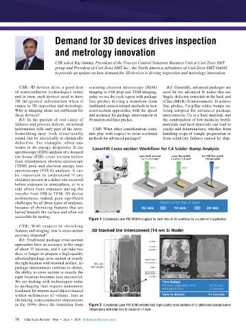
                                           Figure 1: Crossbeam Laser FIB-SEM throughput for each step of the workflow for a customer’s application.
          CSR: With respect to shrinking
        features and imaging, how is cross-section
        accuracy impacted?
          RJ: Traditional package cross-section
        approaches have an accuracy in the range
        of about 15 microns, and it can take two
        days or longer to prepare a high-quality
        advanced-package cross section at exactly
        the right location with minimal artifact. As
        package interconnects continue to shrink,
        the ability to cross section to exactly the
        right location becomes less successful.
        We are dealing with technologies today
        in packaging that require nanometer
        resolution for micron-sized objects located
        within millimeters of volume. Just as
        shrinking semiconductor dimensions
        in the 1990s drove the transition from   Figure 2: Crossbeam Laser FIB-SEM provides fast, high-quality cross sections of Cu-pillar microbumps buried
                                           760µm deep with total time to results of <1 hour.

        38
        38   Chip Scale Review   May  •  June  •  2020   [ChipScaleReview.com]

