Page 38 - ChipScale_May-June_2020-digital
P. 38
is attractive for high bandwidth, low
                                                                              latency, and power saving. 3D-MiM was
                                                                              proposed to be an alternative heterogeneous
                                                                              integration solution to FC-PoP for mobile
                                                                              and 3DIC stacking for high-performance
                                                                              computing (HPC) applications, to realize
                                                                              in-package near-memory computing. For
                                                                              mobile applications, in comparison to
                                                                              the FC-PoP, the 3D-MiM fan-out offers a
                                                                              thinner package profile (~0.5mm z-height),
                                                                              higher data bandwidth (2X~4X), with lower
                                                                              latency (0.2X) and thermal resistance to
                                                                              meet demands of future 5G/AI-driven edge
                                                                              computing. For AI, in comparison to 3DIC
                                                                              HBM, the 3D-MiM fan-out offers a lower
                                                                              cost alternative with a new memory-to-
                                                                              memory, and SoC-to-memory integration
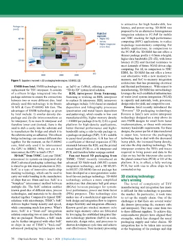
        Figure 1: Suppliers involved in 3D packaging technologies. SOURCE: [2]
                                                                              architecture that has promising electrical
          EMIB from Intel. EMIB technology is a   as InFO or CoWoS, offering a powerful   and thermal performances.  With respect to
        replacement for TSV interposer. It consists   “3D-by-3D” system-level solution.   manufacturing, 3D-MiM fan-out technology
        of a silicon bridge integrated into the   RDL interposer from Samsung.   leverages the well-established infrastructure
        package substrate to ensure the connections   Samsung is working on RDL interposer   of wafer-level system integration (WLSI)
        between two or more different dies. Intel   to replace Si interposer. RDL interposer   in capacity and materials, tools, processes,
        already used this technology in its Stratix   advantages include: 1) It’s based on standard   design rules for yield, and competitive cost.
        10 MX & Core I7-8809G 8th Gen. The   deposition and lithography processes   Foveros. Intel recently introduced the
        advantages of EMIB technology as given   (passivation and metal layers deposition   “Foveros” 3D packaging technology.
        by Intel include: 1) similar density die-  and patterning), which results in low cost   Foveros is Intel’s new active interposer
        package and die-die interconnections as   manufacturability, higher memory density   technology designed as a step above its
        for interposer; 2) no more Si interposer and   > 4 HBM per package (6 to 8); 2) It’s a good   own EMIB designs for small form factor
        therefore lower cost (instead, there is the   platform for high-density applications,   implementations, or those with extreme
        need to etch a cavity into the substrate and   better thermal performance and higher   memory bandwidth requirements. For these
        to manufacture the bridge and attach it to   bandwidth using a side-by-side package vs.   designs, the power per bit of data transferred
        the substrate using an adhesive). This silicon   a package-on-package (PoP); 3) It’s scalable   is super low, however the packaging
        bridge technology can connect different dies   to panel-level production; 4) It has less of   technology has to deal with the decreased
        together. For the moment, on the I7-8809G   a coefficient of thermal expansion (CTE)   bump pitch, the increased bump density,
        core, Intel only used it to interconnect   mismatch between the RDL and the printed   and also the chip stacking technology. The
        the GPU to HBM2. Why not use it to   circuit board (PCB) vs. a Si interposer and   interposer contains the TSVs and traces
        interconnect the GPU to Intel’s CPU?   PCB, and therefore better warpage control  required to bring power and data to the
                 ®
          3D SoIC  from TSMC. Last year TSMC   Fan-out based 3D packaging from   chips on top, but the interposer also carries
        announced its system-on-integrated chip   TSMC. TSMC recently introduced an   the plated contact hole (PCH) or I/O of the
        (SoIC) advanced packaging technology that   advanced 3D Multi-stack (MUST) system   platform. It is, in effect, a fully working
        is slated to go into mass production in 2021.   integration technology, and a 3D MUST-  PCH, but with vias to allow chips to be
        SoIC is a type of innovative multi-chip   in-MUST (3D-MiM) fan-out package has   connected on top.
        stacking technology, which can be used to   been developed as a next-generation wafer-
        carry out wafer bonding in the manufacture   level fan-out package technology. 3D-MiM   3D stacking technology:
        of chips that are 10nm and less. SoIC is a   technology utilizes a more simplified   who’s winning
        “bumpless” interconnect method between   architecture that eliminates ball grid arrays   The level of complexity of TSV
        multiple die. The SoIC solution enables   (BGAs) between packages for system-  manufacturing and integration has made
        known good dies of different sizes, process   level performance, power and form factor   it difficult for this technology to penetrate
        technologies, and materials to be directly   (PPA) purposes. This technology also   the market. In particular, it took time
        stacked together. Compared to typical 3DIC   makes use of a modularized approach for   to set up the supply chain. One of the
        solutions with microbumps, TSMC’s SoIC   both design and integration flow to improve   challenges is that there are several wafer/
        delivers higher bump density and speed,   design flexibility and integration efficiency.   die donors (processing die, memory cube
        while consuming much less power. What’s   Known-good pre-stacked memory cube   and interposer). They may come from two
        more, SoIC is a “front-end” integration   and/or logic-memory cubes are fabricated   to three different suppliers. To achieve this,
        solution connecting two or more dies before   by leveraging the established integrated fan-  semiconductor players have aligned their
        they are packaged. Therefore, a SoIC stack   out technology platform (InFO) in tools,   strengths, which has changed the usual
        can be further integrated with other SoIC   materials, design rules, and processes to   packaging supply and value chains. 3D
        or chips in one of TSMC’s “back-end”   shorten development cycle time and achieve   integration has to be taken into account
        advanced packaging technologies such   cost effectiveness. Near memory processing   at the beginning of the package and chip


        36
        36   Chip Scale Review   May  •  June  •  2020   [ChipScaleReview.com]

