Page 33 - ChipScale_May-June_2020-digital
P. 33
The true cost of undetected defects


        By David L. Adler and Brennan Peterson  [SVXR Inc.]
        T        he cost of an undetected   put together, thereby giving profound   circuit (IC) integration on high-density


                 defect can be much higher
                                           healthcare to transportation.
                 than the cost of the defective   benefits in multiple domains, from   substrates. Figure 1 shows an idealized
                                                                              future assembly, with multiple levels
        part: an electronic component that   Now, however, the issues of integration   of integration. There is, however, one
        fails after installation into a phone, car   become varied in nature when the   lurking issue: integration carries with
        or medical device can cost hundreds,   different manufacturing technologies no   it high costs for failures. The $1 IC
        thousands, or potentially millions of   longer scale as usefully together. It is also   can cause a fail in a $50 board, which
        times the cost of the part. Eliminating   increasingly true that the right DRAM   necessitates a $1000 repair, that in turn
        defects early in the supply chain saves   controller technology is no longer the   might necessitate a $50,000 engineering
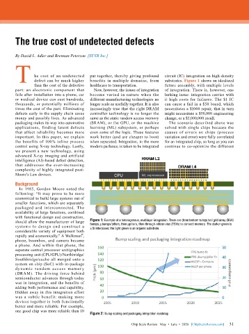
        money and possibly lives. As advanced   same as the static random access memory   change, or a $5,000,000 recall.
        packaging makes its way into automotive   (SRAM), or the GPU, or the machine   The scenario described above was
        applications, finding latent defects   learning (ML) subsystem, or perhaps   solved with single chips because the
        that affect reliability becomes more   even some of the logic. These features   causes of errors on chips (process
        important. In this paper, we explain   work better (and are cheaper to boot)   variation and error) were fully correlated
        the benefits of 100% inline process   when separated. Integration, in the more   for an integrated chip, so long as you can
        control using X-ray technology. Lastly,   modern parlance, is taken to be integrated   continue to co-optimize the different
        we present a new technology, using
        advanced X-ray imaging and artificial
        intelligence (AI)-based defect detection,
        that addresses the ever-increasing
        complexity of highly integrated post-
        Moore’s Law devices.

        Background
          In 1985, Gordon Moore noted the
        following: “It may prove to be more
        economical to build large systems out of
        smaller functions, which are separately
        packaged and interconnected. The
        availability of large functions, combined
        with functional design and construction,
        should allow the manufacturer of large   Figure 1: Example of a heterogenous, multilayer integration. There are (from bottom to top) ball grid array (BGA)
        systems to design and construct a   bumps, µbumps/pillars, then µpillars, then through-silicon vias (TSVs) to connect memory. The darker green is
                                           a Si interposer, the light green is an organic substrate.
        considerable variety of equipment both
                                       ®
        rapidly and economically.” A Walkman ,
        phone, boombox, and camera became
        a phone. And within that phone, the
        separate central processor unit/graphics
        processing unit (CPU/GPU)/Northbridge/
        Southbridge/cache all merged onto a
        system on chip (SoC) with in-package
        dy namic random access memor y
        (DRAM). The driving force behind
        semiconductor advances through today
        was in integration, and the benefits of
        adding both performance and capability.
        Hidden away in this integration effort
        was a subtle benefit: making more
        devices together is both functionally
        better and more reliable. For example,
        one good chip was more reliable than 10
                                           Figure 2: Bump scaling and packaging integration roadmap.

                                                                                                             31
                                                               Chip Scale Review   May  •  June  •  2020   [ChipScaleReview.com]  31

