Page 31 - ChipScale_May-June_2020-digital
P. 31
Deposited copper physical
                                                                              properties
                                                                                Physical properties of the plated copper
                                                                              deposit are essential for the reliability of
                                                                              the substrate. A few of the most important
                                                                              physical properties are tensile strength,
                                                                              elongation percentage,  and internal stress.
                                                                              These properties show the tolerance of the
                                                                              deposit for thermal stress and warpage.
                                                                              Standard testing equipment was used to
                                                                              measure the tensile strength, elongation
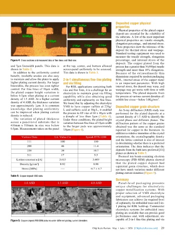
        Figure 4: Cross sections and measured data of fine lines and filled vias.  percentage, and internal stress of the
                                                                              deposit. The copper plated from the
        and 7µm linewidth panels. This data is   at the top, center, and bottom allowed   process has a greater than 36,000psi tensile
        shown in Table 2.                  across-panel uniformity to be assessed.   strength and more than 18% elongation.
          In addition to the uniformity control   This data is shown in Table 3.  Because of the extraordinarily thin
        benefit, insoluble anodes are also easy                               dimensions required by modern packaging
        to maintain and allow the plater to apply   2-in-1 simultaneous fine-line plating   RDL, internal stress of the copper metal
        higher plating current density. For larger   and via filling          is an important parameter. With high
        linewidths, the process has even tighter   For RDL applications containing both   internal stress, the deposit may warp, and
        control. For fine lines of 10µm width,   vias and fine lines, it is a challenge for an   warpage may get worse with time or with
        the plated copper height variation is   electrolyte to maintain great via filling   temperature. The plated deposits from
        below 0.5µm when plating at a current   capability while also obtaining good   the process at various current densities all
        density of 1.5 ASD. At a higher current   uniformity and coplanarity on fine lines.   exhibit low stress—below 1.0Kg/mm .
                                                                                                           2
        density of 4 ASD, the thickness variation   We found that by adjusting the electrolyte
        was approximately 1µm. It is common   VMS to have copper sulfate at 220g/  Deposited copper grain structure
        knowledge that plating uniformity   L and sulfuric acid at 50g/L, it enabled   An X-ray diffraction (XRD) study was
        can be improved when plating current   the process to fill vias of 60 x 40µm with   performed for the plated deposits at a
        density is reduced.                a dimple of less than 5µm (Table 4).   current density of 1.5 ASD to identify the
          The variation of plated thickness   Under these conditions, the plated height   crystal phase and different planes. The
        across a panel-level substrate that is   variation between fine lines of 15µm width   diffraction pattern of the copper grains
        410mm x 510mm in size was below    to the larger pads was approximately   obtained was the same as the standard
        0.5µm. Measurements taken on the panel   1.0µm (Figure 4).            reported for copper in the literature. In
                                                                              addition to relative intensities of the crystal
                                                                              orientations, the crystallographic density
                                                                              and the lattice constant is also of interest
                                                                              in determining whether there is a preferred
                                                                              orientation. The data indicates that the
                                                                              deposits from the bath have preferred [111]
                                                                              planes as shown in Table 5.
                                                                                Focused ion beam-scanning electron
                                                                              microscopy (FIB-SEM) photos showed
                                                                              that the plated copper deposit had
                                                                              equiaxial grain structure, which does
                                                                              not have much variation under different
                                                                              plating current densities (Figure 5).
        Table 5: Copper deposit XRD data.
                                                                              Summary
                                                                                Panel-level  packaging  presents
                                                                              unique challenges for electrolytic
                                                                              copper metallization systems. With
                                                                              proper selection of VMS electrolyte
                                                                              and equipment, advanced packaging
                                                                              fabricators can achieve the required level
                                                                              of coplanarity for embedded trace and 2-in-
                                                                              1 plating for RDL build-up. Commercial
                                                                              electrolyte systems for embedded trace
                                                                              plating are available that can provide good
                                                                              performance and, with adjustment, are
                                                                              capable of 2-in-1 fine-line plating and via
        Figure 5: Copper deposit FIB/SEM pictures under different plating current densities.

                                                                                                             29
                                                               Chip Scale Review   May  •  June  •  2020   [ChipScaleReview.com]  29

