Page 35 - ChipScale_May-June_2020-digital
P. 35
Other costs of quality
          A more practical example for yield
        monitoring would be a case where a few
        months term run at a factory led to partial
        voiding in one of the device interfaces in a
        run of a few thousand devices. Electrically,
        these devices pass, and some will pass a
        stress test.  After longer periods of time,
        however, these devices fail. Because it was
        unmonitored, and concentrated, a number
        of devices will need to be pulled, repaired,
        and a recall issued for items at risk. Even a
        100ppm failure rate on average can lead to
        an expenditure of $20M or more, depending
        on the cost of repair or recall.
          The costs of quality go beyond the
        simple calculation of recalls and returns.
        There are also development cost,
        reputation, product delays, returns (and
        expedition), and time delays on future
        programs. Quality costs are paid for a very
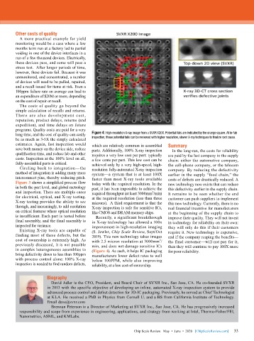
        long time, and the cost of quality can easily   Figure 4: High-resolution X-ray image from a SVXR X200. Potential fails are indicated by the orange square. At in-fab
        be as much as 3-5X the simply calculated   inspection, these potential fails can be reviewed with higher resolution, slower X-ray techniques to finalize root cause.
        estimates. Again, fast inspection would   which are relatively common in assembled   Summary
        save both money on the device side, reduce   parts. Additionally, 100% X-ray inspection   In the long-run, the costs for reliability
        qualification time, and reduce lab and other   requires a very low cost per part: typically   are paid by the last company in the supply
        costs. Inspection at the 100% level on all,   a few cents per part. This low cost can be   chain: either the automotive company,
        fully-assembled parts is critical.  achieved only by a very high-speed, high-  the cell-phone company, or the telecom
          Circling back to integration—the   resolution fully-automated X-ray inspection   company. By reducing the defectivity
        method of integration is adding many more   system—a system that is at least 100X   earlier in the supply “food chain,” the
        interconnect pins, thereby reducing pitch.   faster than most X-ray tools available   costs of defects are drastically reduced. A
        Figure 3 shows a simplified process flow   today with the required resolution. In the   new technology now exists that can reduce
        in both the part level, and global metrology   past, it has been impossible to achieve the   this defectivity earlier in the supply chain.
        and inspection. There are multiple cases   required throughput (at least 3000mm /min)   It remains to be seen whether the end
                                                                       2
        for electrical, optical, and X-ray testing.   at the required resolution (less than three   customer can push suppliers to implement
        X-ray testing provides the ability to see   microns).  A third requirement is that the   this new technology. Currently, there is no
        through, and increasingly, to add resolution   X-ray inspection is safe for sensitive ICs,   real financial incentive for manufacturers
        on critical features where optical resolution   like CMOS and DRAM memory chips.  at the beginning of the supply chain to
        is insufficient. Each part is tested before   Recently, a significant breakthrough   improve their quality. They will not invest
        final assembly, and the final assembly is   in X-ray technology has allowed a 100x   in technology for reliability on their own:
        inspected for variance.            improvement in high-resolution imaging   they will only do this if their customers
          Existing X-ray tools are capable of   (S. Jewler, Chip Scale Review, Sept/Oct   require it. New technology is expensive,
        finding most of these defects, but the   2019). This new technology takes images   and if the company reaping the benefits—
        cost of ownership is extremely high. As   with 2.5 micron resolution at 3000mm /  the final customer—will not pay for it,
                                                                           2
        previously discussed, it is not possible   min, and does not damage sensitive ICs   then they will continue to pay 100X more
        in complex heterogeneous assemblies to   (Figure 4). As such, it helps IC packaging   for poor reliability.
        bring defectivity down to less than 100ppm   manufacturers lower defect rates to well
        with process control alone: 100% X-ray   below 100PPM, while also improving
        inspection is needed to find random defects,   reliability, at a low cost-of-ownership.


                       Biography
                         David Adler is the CEO, President, and Board Chair of SVXR Inc., San Jose, CA. He co-founded SVXR
                       in 2013 with the specific objective of developing an inline, automated X-ray inspection system to provide
                       advanced process control and defect detection for 3D-IC packaging. Previously, he served as Chief Technologist
                       at KLA. He received a PhD in Physics from Cornell U. and a BS from California Institute of Technology.
                       Email dave@svxr.com
                         Brennan Peterson is a Director of Marketing at SVXR Inc., San Jose, CA. He has progressively increased
          responsibility and scope from experience in engineering, applications, and strategy from working at Intel, Thermo-Fisher/FEI,
          Nanometrics, ASML, and KMLabs.


                                                                                                             33
                                                               Chip Scale Review   May  •  June  •  2020   [ChipScaleReview.com]  33

