Page 28 - ChipScale_May-June_2020-digital
P. 28
Embedded trace and 2-in-1 RDL for fan-out


        panel-level packaging


        By Kesheng Feng, Kwangsuk Kim, Saminda Dharmarathna, William Bowerman, Jim Watkowski, Johnny Lee, Jordan Kologe
        [MacDermid Alpha Electronics Solutions]
        W            ith respect to fan-out   SAP has been used for making fine lines   mSAP f low  begins  with  an  organic


                     panel-level packaging
                                           process begins with electroless copper
                                                                              foil of approximately 1-5µm in thickness.
                     (FOPLP), fabricators   on organic substrates for decades. The   substrate clad with a very thin copper
        have struggled to justify the upfront   plating to form an ultra-thin conductive   Microvias are then laser drilled and the
        costs of installing the process because   seed layer, followed by photolithography   panels desmeared, either through a plasma
        of challenges with copper plating   to pattern a photo resist on the surface.   or chemical desmear or a combination
        performance and package cost reduction   Electrolytic copper plating is then used   of both. This process cleans any resin
        compared to fan-out wafer-level packaging   to form metallization structures between   residues from the target pad and imparts
        (FOWLP). A key challenge is obtaining   the photo resist patterns. This is then   topography to the via walls for adhesion
        a combination of high line resolution   followed by removal of photo resist   of subsequent copper deposits. The
        and height uniformity from the copper   and flash etching away the copper seed   panels are then processed through a
        plating process that forms the circuitry   layer to complete the patterning. SAP   primary metallization process such as,
        of the redistribution layer (RDL). This is   has advanced enough to allow wiring   electroless copper, carbon-based direct
        especially challenging in simultaneous   dimensions down to 9μm, but due to the   metallization, or conductive polymer,
        plating of traces and filling of vias, in   small amount of side etching that occurs   to make the via walls conductive for
        what is called 2-in-1 (RDL) plating.   to the plated copper traces during the flash   electrolytic copper plating. The panels are
        Coplanarity between the surface of the   etching step, there has been a challenge in   subsequently imaged and pattern-plated
        plated copper traces, pads and/or filled   reducing linewidth scales further. There   with electrolytic copper to both fill the
        vias is a critically important qualifying   are also other challenges as line/space   microvias completely with copper, and
        feature for these copper plating processes.   trends approach 9µm/9µm, including   build the copper traces to the required
        A surface that is not coplanar could   adhesion to the organic substrate, process   height in a single step. After plating, the
        result in signal transmission loss and   tool accuracy across uneven substrate   resist is stripped and a differential or flash
        distortion of the circuitry layers after   surfaces on panels that can be in the   etch is done to form the final circuitry. The
        lamination. These defects can cause   range of 500mm x 400mm in size, plating   fine-line resolution from this technology is
        short circuiting and catastrophic failure   thickness uniformity, and the high costs of   typically limited to 13µm dimensions.
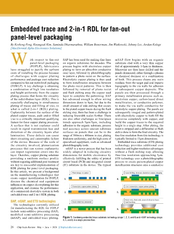
        of the device. Because of the scale of   specialized equipment, such as advanced   Embedded trace substrate (ETS) plating
        the circuitry involved, planarization   photolithography tools.       technology provides additional cost
        processes that can restore coplanarity   mSAP is a newer process that has been   reduction and higher resolution advantages
        can impart registration errors into the   widely adapted in reducing circuitry   without a flash etching step, allowing
        layer. Therefore, copper plating solutions   dimensions for mobile electronics by   fine-line resolution approaching 5µm.
        providing a uniform surface profile   effectively fulfilling the utility of printed   ETS technology uses a photolithographic
        without requiring additional post treatment   circuit board (PCB) and integrated circuit   process to create pattern-plated copper
        are key to successful implementation of   (IC) substrate in the device. The typical   metallization structures onto a conductive
        RDL plating for panel-level packaging.
        In this article, we present a background
        on the manufacturing technologies that
        create copper metallization for FOPLP,
        discuss the chemical and equipment
        influences on copper electroplating for this
        application, and examine the performance
        of a commercial electrolyte system in both
        embedded trace and 2-in-1 RDL plating.

        SAP, mSAP, and ETS technologies
          The technologies currently utilized
        for manufacturing the RDL for FOPLP
        include semi-additive processing (SAP),
        modified semi-additive processing
        (mSAP), and embedded trace plating.   Figure 1: Combining embedded trace substrate technology (steps 1, 2, 3, and 6) and mSAP technology (steps
                                           4, 5, and 6) in a single process flow.

        26
        26   Chip Scale Review   May  •  June  •  2020   [ChipScaleReview.com]

