Page 19 - Chip Scale Review_January-February_2024-digital
P. 19
b ot h sid e ef f icie nt me t a l l ic
            t her m a l i nter f a c e m a ter ia l s
            (TIM), reduced die-die thermal
            resistance, and thermal cross-talk
            between neighboring die.
          •  Handling higher power density
            with a thermally-efficient Si floor
            plan.

          ELAIC physical characterization.
        We used a variety of nondestructive
        a n a ly si s t e ch n iq u e s fo r E L A IC
        physical device characterization.
        Figures 4 -5 show representative
        examples of ELAIC characterization.
        S E M , c o n f o c a l s c a n , X - r a y ,
        a n d o p t ic a l i m a ge s a r e u s e d t o
        characterize  key  fabrication  steps,
        which include chip-to-chip spacing,
        i nt e r- c h i p  pl a n a r it y,  d iele c t r ic
        deposition, via formation, feature
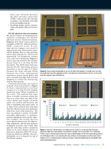
        size, and micro-bumping.  Figure 4
        shows  spacing  between the stealth-
        diced chips i n a 16 - chip ELA IC
        assembly. The SEM data indicates
        that the ELAIC fabrication process
        maintains a narrow gap of 5-20µm
        between  the chips and gap filling   Figure 6: Passive circuit demonstration on top of a 16-chip ELAIC assembly: a) A single metal layer RDL;
        b et we e n t he ch ips. Ap propr iat e   b) A double metal layer RDL deposited on BCB; c-d) A daisy chain circuit created on top of a 16-chip ELAIC
        cleaning to remove dicing debris and   assembly using multi-layer BCB dielectric.
        give a smooth chip edge with minimal
        chipping is critical for minimizing
        chip-to-chip spacing.
          Confocal microscopy was used to
        evaluate inter-chip planarity. Figure
        5  shows represent ative confocal
        images  of  a  4-chip  ELAIC  module
        measured using 100nm resolution in
        the z-axis. The confocal line scans
        show z-height variation along the
        line as it scans from one chip to the
        other. Metal pad height variation
        (pad 1-6) within and between the
        chip is negligible (less than 1µm).  It
        is clear from confocal line scan data
        that the fabrication process maintains
        chip-like inter-chip planarity. We
        have developed a variety of ELAIC
        assembly approaches to optimize
        critical alignments between the chips.
        For example, the ELAIC devices
        used optical microscope for chip-to-
        chip alignment, and the post-process
        alignment accuracy was ±3µm. The
        gap fill and chip surface planarity
        allow us to select from a variety of   Figure 7: A passive interconnection circuit demonstration on top of a 16-chip assembly. The figure
        dielectric  material  (PECVD  oxide,   represents single-metal-layer passive circuits with four sections. Each 4-chip section has 1-10µm wide,
        benzocyclobutene [BCB], silicone,   5-20mm long circuit traces going between the chips. a) Optical image of ELAIC and corresponding selective
        polyimide, etc.) to deposit on top of   area SEM images of the circuit connecting the chips; b) Measured room temperature (RT) passive circuit
        the ELAIC surface.                 resistance for four different sections. Resistance variation is due to the different widths and lengths of the
                                           electrical interconnect lines.

                                                                                                             17
                                                          Chip Scale Review   January  •  February  •  2024   [ChipScaleReview.com]  17

