Page 17 - Chip Scale Review_January-February_2024-digital
P. 17
(PECVD) silicon dioxide layer, polyimide, or BCB     for chip-to-chip communication. This approach requires
        dielectric, and uses micro-vias for interconnection. For our   small electrical length and more individual physical wires
        demonstration, the metal wiring layers were patterned using   for data transmission. ELAIC enables narrow chip-to-
        non-contact direct-write photolithography, which supports   chip spacing (10-20x smaller than the traditional approach)
        minimum wiring layer dimensions of 1µm and field sizes   for smaller interconnect lengths and finer feature circuits,
                                                    2
        exceeding the largest relevant reticle size (50 x 50mm ).   thereby enabling more physical wires for I/O connections
          We evaluated  various chip-like  dielectric, wiring,   with lower-latency, lower-power, higher-bandwidth chip-to-
        and interconnection options. An ELAIC process flow is   chip communication.
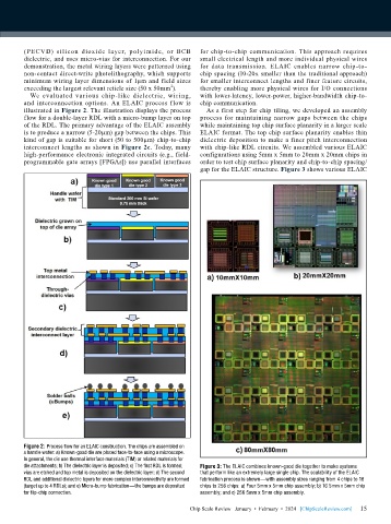
        illustrated in Figure 2. The illustration displays the process   As a first step for chip tiling, we developed an assembly
        flow for a double-layer RDL with a micro-bump layer on top   process for maintaining narrow gaps between the chips
        of the RDL. The primary advantage of the ELAIC assembly   while maintaining top chip surface planarity in a larger scale
        is to produce a narrow (5-20µm) gap between the chips. This   ELAIC format. The top chip surface planarity enables thin
        kind of gap is suitable for short (50 to 500µm) chip-to-chip   dielectric deposition to make a finer pitch interconnection
        interconnect lengths as shown in Figure 2c. Today, many   with chip-like RDL circuits. We assembled various ELAIC
        high-performance electronic integrated circuits (e.g., field-  configurations using 5mm x 5mm to 20mm x 20mm chips in
        programmable gate arrays [FPGAs]) use parallel interfaces   order to test chip surface planarity and chip-to-chip spacing/
                                                             gap for the ELAIC structure. Figure 3 shows various ELAIC


        Figure 2: Process flow for an ELAIC construction. The chips are assembled on
        a handle wafer: a) Known-good die are placed face-to-face using a microscope.
        In general, the die use thermal interface materials (TIM) or related materials for
        die attachments; b) The dielectric layer is deposited; c) The first RDL is formed;   Figure 3: The ELAIC combines known-good die together to make systems
        vias are etched and top metal is deposited on the dielectric layer; d) The second   that perform like an extremely large single chip. The scalability of the ELAIC
        RDL and additional dielectric layers for more complex interconnectivity are formed   fabrication process is shown—with assembly sizes ranging from 4 chips to 16
        (target up to 4 RDLs); and e) Micro-bump fabrication—the bumps are deposited   chips to 256 chips: a) Four 5mm x 5mm chip assembly; b) 16 5mm x 5mm chip
        for flip-chip connection.                            assembly; and c) 256 5mm x 5mm chip assembly.

                                                                                                             15
                                                          Chip Scale Review   January  •  February  •  2024   [ChipScaleReview.com]  15

