Page 21 - Chip Scale Review_January-February_2024-digital
P. 21
I-V characteristic of Nb/Al-AlOx/
        Nb unshunted tunnel junctions (i.e.,
        with respect to the Josephson critical
        cur rent, sub-gap voltage, nor mal
        resistance at 4.2K). A variety of
        active superconducting chips with tri-
        layer junctions have been assembled
        to implement the ELAIC. The I–V
        characteristics and switching current of
        various tri-layer flip-chip JJ arrays were
        measured. We measured many ELAIC
        JJ arrays ranging from 40 to 20,000
        JJs in series, with JJ drawn diameters
        ranging  between  1.0μm  and  0.7μm.
        I-V characteristics were measured for
        ELAIC JJ arrays connected across
        multiple chips through the R DL.
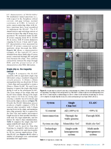
        Figure 8d shows a representative
        example of the typical I-V cur ve
        obtained from these multi-chip JJ series
        arrays connected through Nb and gold
        lines between the chips. This confirms
        connectivity between the chips through
        R DL a nd t he pre se r vat ion of JJ
        characteristics after RDL fabrication.
        Single chip vs. the megachip
        concept
          Figure 9 compares the ELA IC
        assembly with an equivalent single chip
        fabricated using a standard integrated
        circuits process. A 20mm x 20mm
        unsingulated chip was diced into 16 5mm
        x 5mm chips and reassembled to create a
        20mm x 20mm ELAIC. We used X-ray
        imaging to inspect the single chip before
        dicing as well as the subsequent ELAIC.   Figure 9: A single-chip vs. an ELAIC assembly: a) Optical image of a 20mm x 20mm unsingulated chip; and b)
        The X-ray image of the single chip and   corresponding X-ray image of that unsingulated chip. This 20mm x 20mm single chip was subsequently diced
        ELAIC looks similar. Dicing of the single   into 16 5mm x 5mm chiplets. c) Optical image of a 20mm x 20mm ELAIC formed by recombining the 16 5mm
        chip removes Si from the dicing lane   x 5mm chiplets into single chip-like structures; and d) corresponding X-ray image of the ELAIC in c).
        causing a smaller metal-to-metal gap
        between the chips as shown in Figure 9d.
        Overall, the ELAIC fabrication process
        produces a highly compact (>99% Si
        content) chip assembly with 5-20μm
        spacing between the chips, and maintains
        inter-chip planarity that is required for
        the finer line and smaller interconnect
        length needed to form parallel interfaces
        with wide I/O, high-bandwidth, and low
        latency for chip-to-chip communication.
        Table 1 compares the single-chip SoC
        option with ELAIC multi-die SoC.
          ELAIC  can  be used  for  f lip-chip
        bonding to simplify fabrication and
        enhance connectivity and functionality
        in 3D for various applications. Flip-
        chip ELAIC (see Figures 10-11) offers a
        number of advantages over conventional
        monolithic SoC approaches:
                                           Table 1: A megachip vs. a single chip.

                                                                                                             19
                                                          Chip Scale Review   January  •  February  •  2024   [ChipScaleReview.com]  19

