Page 18 - Chip Scale Review_January-February_2024-digital
P. 18
configurations using 5mm by 5mm
        chips ranging from 4 chips up to 256
        chips as a representative example.
        The extremely large area (Figure
        3c, 80mm by 80mm) circuits can be
        useful for advancing many systems,
        including those for HPC with diverse
        technology nodes for AI and deep
        learning, superconducting classical
        and quantum computing, large-format
        digital-pixel focal plane arrays [15-17]
        with minimum seam loss, photonic-
        chip tiling, millimeter-wave phased-
        array radar tiles, etc. The process
        involves  the tiling of known-good
        chips to make systems that perform
        like a single-chip monolithic device,
        despite actually being composed of
        several smaller heterogeneous chips.
        Integration of multiple chips with
        different (heterogeneous) fabrication
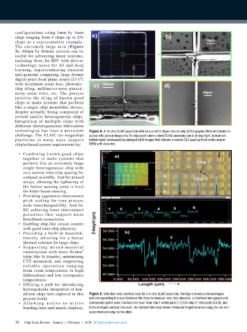
        technologies has  been a persistent   Figure 4: A 16-chip ELAIC assembly with very small 5-20µm chip-to-chip (C2C) spacing filled with dielectric.
        challenge. The ELAIC (or megachip)   a) (top left): optical image of a 16-chip (each 5mm x 5mm) ELAIC assembly and b-d) (top right, bottom left,
        platfor ms in many ways suppor t   bottom right) corresponding enlarged SEM images that indicate a narrow C2C spacing filled (white area in
        chiplet-based system requirements by:  SEM) with dielectric.
          •  Combining known-good chips
            together to make systems that
            perform like an extremely large
            single  heterogeneous  chip with
            very narrow inter-chip spacing for
            compact assembly. And for phased
            arrays, allowing the tightening of
            the lattice spacing (area is less)
            for better beam-steering.
          •  Providing aggressive interconnect
            pitch scaling for true process
            node interchangeability. And for
            RF, achieving lower interconnect
            pa rasit ics that suppor t more
            broadband connections.
          •  Enabling chip-like circuit content
            with good inter-chip planarity.
          •  Providing a built-in heatsink,
            thereby allowing for a better
            thermal solution for large chips.
          •  S u p p or t i n g  m i xe d -m at e r i a l
                                        3
            construction with more Si/mm
            (chip-like Si density), minimizing
            CTE mismatch, and supporting
            r el i a b l e  o p e r a t io n  r a n g i n g
            from  room temperature to  high
            (fabrication) and low (cryogenic)
            temperatures.
          •  Offering a path for introducing
            heterogeneous integration of non-
            silicon chips (not explored in this   Figure 5: Selective-area confocal scan for a 4-chip ELAIC assembly. The figure shows confocal images
            present work).                 and corresponding line scan between the chips to measure inter-chip planarity: a) Confocal micrograph and
          •  A l l ow i n g  a c t i ve - t o - a c t i ve   corresponding line scan. Confocal line scan from chip 1 metal pads (1,2,3) to chip 2 metal pads (4,5,6); and
            bonding (mix-and-match chiplets),   b) An enlarged confocal line scan; the confocal line scan shows metal pad height variation along the line as it
                                           scans from one edge to the other.

        16
        16   Chip Scale Review   January  •  February  •  2024   [ChipScaleReview.com]

