Page 20 - Chip Scale Review_January-February_2024-digital
P. 20
ELAIC electrical interconnect    at 4K. To quantify the effects of    To assess the electrical performance
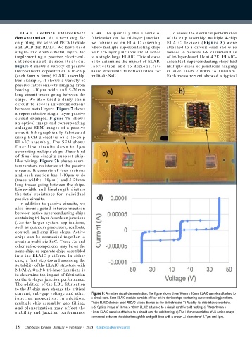
        demonstration. As a next step for   fabrication on the tri-layer junction,   of the chip assembly, multiple 4-chip
        chip tiling, we selected PECVD oxide   we fabricated an ELAIC assembly   ELA IC devices ( Fig ure 8) were
        and BCB for RDLs. We have used     where multiple superconducting chips   attached to a circuit card and wire
        single- and double-metal layers for   with tri-layer junctions are attached   bonded to measure I-V characteristics
        implementing a passive electrical-  to a single large ELAIC. This allowed   of tri-layer-based JJs at 4.2K. ELAIC-
        i n t e r c on n e c t  d e m on s t r at i on .   us to determine the impact of ELAIC   assembled superconducting chips had
        Figure 6 shows a variety of passive   f a b r ic a t io n a n d t o d e mo n s t r a t e   multiple sizes of junctions ranging
        interconnects deposited on a 16-chip   basic desirable functionalities for    i n si ze f rom 70 0 n m to 10 0 0 n m.
        (each 5mm x 5mm) ELAIC assembly.   multi-die SoC.                     Each measurement showed a typical
        For example, it shows a variety of
        passive interconnects ranging from
        having  1-10µm  wide  and  5-20mm
        long circuit traces going between the
        chips. We also used a daisy chain
        circuit to access interconnections
        between metal layers. Figure 7 shows
        a representative single-layer passive
        circuit  example.  Figure  7a    shows
        an optical image and corresponding
        enlarged  SEM  images  of  a  passive
        circuit lithographically-fabricated
        using BCB dielectric on a 16-chip
        ELAIC assembly. The SEM shows
        f i ner li ne ci rcu it s dow n to 1µm
        connecting multiple chips. These kind
        of  fine-line  circuits support  chip-
        like wiring. Figure 7b shows room-
        temperature resistance of the passive
        circuits. It consists of four sections
        and each section has 1-10µm wide
        (trace width:1-10µm ) and 5-20mm
        long traces going between the chips.
        Linewidth  and  linelength  dictate
        the total resistance for individual
        passive circuits.
          In addition to passive circuits, we
        also  investigated  interconnection
        between active superconducting chips
        containing tri-layer Josephson junctions
        (JJs) for larger system applications,
        such as quantum processors, readouts,
        control, and amplifier chips. Active
        chips can be connected together to
        create a multi-die SoC. These JJs and
        other active components may be on the
        same chip, or separate chips assembled
        into the ELAIC platform. In either
        case, a first step toward assessing the
        suitability of the ELAIC structure with
        Nb/Al-AlOx/Nb tri-layer junctions is
        to determine the impact of fabrication
        on the tri-layer junction performance.
        The addition of the RDL fabrication
        to the JJ chip may change the critical
        current, sub-gap voltage and other   Figure 8: An active circuit demonstration. The figure shows three 10mm x 10mm ELAIC samples attached to
        junction proper ties. In addition,   a circuit card. Each ELAIC module consists of four active device chips containing superconducting junctions.
        multiple chip assembly, gap filling,   These ELAIC devices used PECVD silicon dioxide as the dielectric and Ti-Au chip-to-chip interconnections.
        and planarization may affect the   a-b) Optical image of 10mm x 10mm ELAIC attached to a circuit card for cold testing; c) Three 10mm x
        stability and junction performance   10mm ELAIC samples attached to a circuit card for cold testing; d) The I-V characteristics of JJ series arrays
                                           connected between the chips through Nb and gold lines with a drawn JJ diameter of 0.7μm and 1μm.

        18   Chip Scale Review   January  •  February  •  2024   [ChipScaleReview.com]
        18

