Page 22 - Chip Scale Review_January-February_2024-digital
P. 22
•  Provides various low-cost multi-
                                                                                  chip read-out IC (ROIC) assembly
                                                                                  for silicon avalanche photodiodes
                                                                                  (Si-APDs) and other imagers [15-17].
                                                                                •  Introduces flip-chip Si-less active/
                                                                                  passive bridge for chip-to-chip
                                                                                  connection.
                                                                                •  Enables a thermally-optimized Si
                                                                                  floorplan.
                                                                                •  Provides a cost benefit for yield and
                                                                                  node optimization.

                                                                              Summary
                                                                                An integrated approach to develop
                                                                              ELAICs, or “megachips,” using various
                                                                              heterogeneous die configurations has
                                                                              been demonstrated. This approach
                                                                              is suitable for high-end, expensive
                                                                              electronics where an SoC can be
                                                                              divided into chiplets with desired
                                                                              functionality and an ELAIC multi-
                                                                              die SoC can be created. The ELAIC
                                                                              can incorporate chips/chiplets from
                                                                              different foundr y processes, and
                                                                              different technology nodes to improve
                                                                              mix and match capability, which
                                                                              further improves package performance.
                                                                              It also provides scalability to place a
                                                                              large number of chips onto the ELAIC
                                                                              platform, and enables a design that
                                                                              packages many different functionalities
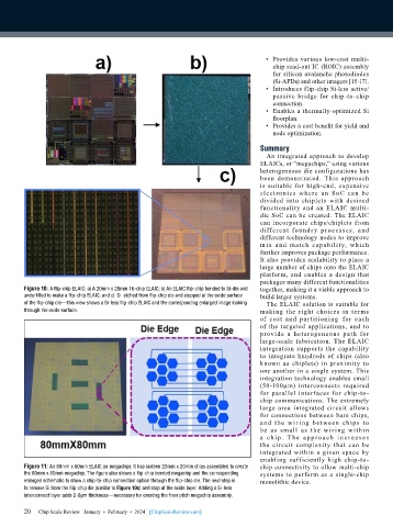
        Figure 10: A flip-chip ELAIC: a) A 20mm x 20mm 16-chip ELAIC; b) An ELAIC flip-chip bonded to Si-die and   together, making it a viable approach to
        underfilled to make a flip-chip ELAIC; and c)  Si  etched from flip-chip die and stopped at the oxide surface   build larger systems.
        of the flip-chip die—this view shows a Si-less flip-chip ELAIC and the corresponding enlarged image looking   The ELAIC solution is suitable for
        through the oxide surface.                                            making the right choices in terms
                                                                              of cost and partitioning–for each
                                                                              of the targeted applications, and to
                                                                              provide a heterogeneous path for
                                                                              large-scale fabrication. The ELAIC
                                                                              integration supports the capability
                                                                              to integrate hundreds of chips (also
                                                                              known as chiplets) in proximity to
                                                                              one another in a single system. This
                                                                              integration technology enables small
                                                                              (50-100µm) interconnects required
                                                                              for parallel interfaces for chip-to-
                                                                              chip communications. The extremely
                                                                              large  area  integrated  circuit  allows
                                                                              for connections between bare chips,
                                                                              and the wir ing bet ween chips to
                                                                              be as small as the wiring within
                                                                              a ch ip. T he a p p r oa ch i nc r e a s e s
                                                                              the circuit complexity that can be
                                                                              integrated within a given space by
                                                                              enabling sufficiently high chip-to-
        Figure 11: An 80mm x 80mm ELAIC (or megachip). It has sixteen 20mm x 20mm chips assembled to create   chip connectivity to allow multi-chip
        the 80mm x 80mm megachip. The figure also shows a flip-chip bonded megachip and the corresponding   systems to perform as a single-chip
        enlarged schematic to show a chip-to-chip connection option through the flip-chip die. The next step is   monolithic device.
        to remove Si from the flip-chip die (similar to Figure 10c) and stop at the oxide layer. Adding a Si-less
        interconnect layer adds 2-6µm thickness—necessary for creating the finer pitch megachip assembly.

        20
        20   Chip Scale Review   January  •  February  •  2024   [ChipScaleReview.com]

