Page 16 - Chip Scale Review_January-February_2024-digital
P. 16
layers (RDLs), active interposers,   node tech nolog y beyond what is   array), the ELAIC approach can help
        a nd br idge d ie have become t he   possible in a single-chip format.   solve many scalability challenges for
        prefer red methods for lower-cost    A key focus of this paper is to   high-end electronics.
        integration to meet the demands of   address the scaling challenges faced
        higher functionality in ever-smaller   when building large-scale processors.   The megachip approach
        packages, especially when coupled   For example, the ELAIC solution is   The following sections discuss
        with the use of different technology   suitable for combining multiple types   the megachip (or ELAIC) approach
        node die [11-13]. The size of WLP   of chips (e.g., memory, ASICs, CPUs,   w it h r e s p e c t t o t i l i ng, physica l
        increases with smaller technology   GPUs, power conditioning) into a   characterization, and demonstration of
        nodes and causes more reliability   single system. This approach extends   the electrical interconnect.
        and chip package mismatches. Today,   the number of chip tiles within a   ELA IC  chip -t i l ing  approach.
        various WLP technologies including   given space by enabling sufficiently   The approach to ELAICs involves
        WLPs with and  without through-    high chip-to-chip connectivity to   developing an integration process
        sil icon v ia s (TSVs), W LPs w it h   allow multiple chiplets to perform   t h a t c a n a d d r e s s t h e s c a l i ng
        embedded-integrated passive devices,   as a single-chip monolithic device.   challenges faced by many multi-
        and use of low CTE, low-loss, high-  Con necting chiplets th rough our   chip systems. Integration of multiple
        glass  transition  temperature  (Tg)     approach will enable a path to increase   ch ips t h at we re pro duce d u si ng
        material-based wafer-level substrates   the for mat size of heterogeneous   different (heterogeneous) fabrication
        featuring fine traces and embedded/  processors. The ELAIC structure,   technologies has been a persistent
        i nteg rated passives, a re used to   having 5-20μm chip-to-chip spacing,   challenge. Typically, individually-
        reduce WLP chip package mismatch.   c r e a t e s  sho r t  ( i . e . ,  5 0 -5 0 0 μ m)   packaged chips use a board-level
        Similarly, flip-chip integration with   electrical links for high-bandwidth,   assembly approach, and the associated
        the bridge die embedded within the   low-latency com mu n icat ion. A n   “parasitic” electrical overhead and
        package substrate allows for shorter   ELAIC has a chip-like silicon content   latency often become the limiting
        interconnect lengths for chip-to-chip   (about 99%), allowing thermally-  factors to a system’s performance.
        communication. Active interposers   stable and inexpensive fabrication   The ELAIC integration process will
        with active-to-active bonding [14]   of a heterogeneous SoC with chip-  allow the tiling of known-good chips
        are preferred for high-bandwidth,    like wiring densities. For HPC, power   to make systems that perform as a
        low-latency communication.         consumption comes primarily from   single-chip monolithic device, despite
          Although there are many packaging   movi ng d at a bet ween ch ips i n a   being composed of several smaller
        approaches available today for chiplet   system rather than from the on-chip   heterogeneous chips. The primary
        integration, the authors believe that   computing operations. The ELAIC   goal of this effort is to develop a chip
        there is room for further improvement.   approach reduces data movement   packaging interconnected with a RDL
        Til i ng hu nd red s of k now n-good   constraints by  integrating  multiple   that is capable of integrating hundreds
        chips in proximity to one another   chiplets with minimum chip-to-chip   of chips in proximity to one another in
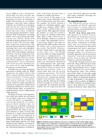
        and creating chip-like wiring and   spacing, thereby reducing the loading   a single system as shown in Figure 1.
        silicon content are highly desirable for   of these I/O paths by at least an order   The RDL typically has multiple metal
        creating next-generation chiplet-based   of magnitude. By integrating multiple   layers, each separated by a plasma-
        computing architectures, but has yet to   chiplets into one large-area chip (2D   enhanced chemical vapor deposition
        be demonstrated. Here, we present the
        implementation of such a chiplet-based
        tiling approach.
          This paper discusses a heterogeneous
        chip tiling that enables the realization
        of extremely large-area integrated
        circuits (ELAICs)—or megachips—
        c o nt a i n i ng  hu nd r e d s  of  clo s ely
        s p a c e d s m a l l c h i p l e t s t h a t a r e
        interconnected using RDLs fabricated
        via a lithographic process. The ELAIC
        platform allows the tiling of known-
        good chiplets to make systems that
        perform as a single-chip monolithic
        device,  despite being composed  of
        many smaller heterogeneous chiplets.
        With this approach, one can fabricate a
        large-format single-chip-like SoC from   Figure 1: Extremely large-area integrated circuit (ELAIC), or megachip, concept: a) (left) Regular package
        advanced-node chiplets, screening for   where individual chips are attached to the substrate (organic or Si) and interconnected through the substrate;
        known-good die in order to increase   b) The megachip combines all the chips in a single plane where each individual chip will have at least two
        the yield and performance of advanced-  nearest neighbor chips for interconnection. The megachip enables chip-like wiring and eliminates the need for a
                                           substrate containing interconnects.

        14   Chip Scale Review   January  •  February  •  2024   [ChipScaleReview.com]
        14

