Page 23 - Chip Scale Review_March April_2023-digital
P. 23
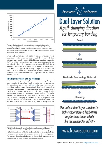
Figure 2: Typical die size for high-end microprocessors including graphics
        processing units (GPUs) as a function of year of introduction. For reference, the
                                          2
        Intel Pentium introduced at the 0.8μm node was 300mm  and had about 3 million
        transistors. In 2021, the Nvidia A100 made at the TSMC 4N node was about 836mm   2
        with about 54 billion transistors.
        layer and requiring only nearest neighbor connections
        (sometimes called a systolic architecture). However, both these
        attempts employed a monolithic bipolar junction transistor
        (BJT) or CMOS technology and could not, for example, use
        high-density dynamic random access memory (DRAM) for its
        memory. Another thing to remember is something called Rent’s
        rule. This rule suggests that as chip complexity increases, the
        number of I/Os should also increase as the more complex larger
        chip would need to send and receive larger amounts of data with
        lower latencies.

        Tackling the package scaling challenge
          Because package scaling has not kept up, chip designers
        have resorted to serializers and de-serializers to get around
        the problem. As shown in  Figure 3, many signals are
        serialized and sent over the relatively few board channels at
        extremely high speed. We are reaching data rates of over a
        100Gb/s per channel. However, sending signals at this high
        rate presents several challenges that result in these I/Os taking
        up more real estate (as high as 30-40%, or even more, of the
        chip area) and using up to 30-40% of the chip’s power (chip
        area and power are correlated). This is unsustainable—and
        the poor control of wires on a PCB, surface roughness and


        Figure 3: Inter-die signals can be handled in two different ways: a) Because of
        fewer inter-chip connections on PCBs, signals are serialized and sent at high speed
        over transmission lines on a PCB. They are deserialized at the receiving chip. These
        SerDes are large and complex and can consume as much as 40% of the chip power. b)
        If we had more wires between the dies, and the dies are closely spaced, we can send
        the native signals as-is over wires that resemble wires on a chip.

                                                                                                             21
                                                             Chip Scale Review   March  •  April  •  2023   [ChipScaleReview.com]  21

