Page 20 - Chip Scale Review_March April_2023-digital
P. 20
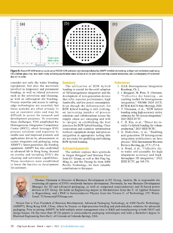
Figure 5: Recent DP-D2W bonding results using EVG320 D2W activation and cleaning followed by ASMPT LithoBolt die bonding: a) Alignment verification result using
        COG (9x9mm glass chip), face-down mode; achieving specification below 200nm at 3σ; b) post-bond scanning acoustic microscope; and c) photography of the bonded
        dies on the wafer.
        consider not only the wafer bonding   Summary                         References
        equipment, but  also the materials   The utilization of D2W hybr id     1.  IEEE Heterogeneous Integration
        involved in temporary and permanent   bonding is crucial for the swift adoption   Roadmap, Ch. 2.
        bonding, as well as related processes   of 3D/heterogeneous integration and the   2.  J. Burggraf, M. Pires, T. Uhrmann,
        such as die activation and cleaning,   development of next-generation devices   “Collective die bonding - an
        as well as subsequent die bonding.   that offer superior performance, high   enabling toolkit for heterogeneous
        Process expertise and access to cutting-  bandwidth, and low power consumption.   integration,” PRiME 2020 (ECS,
        edge technologies are essential, but   Even though the infrastructure for   ECSJ & KECS Joint Meeting), 2020.
        these systems are often already in   D2W hybrid bonding is still evolving,   3.  T. Uhrmann, et al., “D2W hybrid
        use at customer sites and may be   an increasing number of process         bonding using high-accuracy carrier
        difficult to access for research and   solutions and collaborations across the   solutions for 3D system integration,”
        development purposes. To overcome   supply chain are emerging and will     2023 IEEE ECTC.
        these challenges, EVG established the   be integral in establishing the best   4.  C. H. Fan, et al., “Direct die-to-
        Heterogeneous Integration Competence   practices for D2W hybrid bonding. Close   wafer Cu hybrid bonding for volume
        Center (HICC), which leverages EVG   cooperation and seamless optimization   production,” 2023 IEEE ECTC.
        process solutions and expertise to   between equipment design and process   5.  A. Elsherbini, et al., “Enabling
        enable new and improved products and   integration in appropriate testing labs   next-generation 3D heterogeneous
        applications driven by advancements in   are necessary for qualifying and refining   integration architectures on Intel
        system integration and packaging, using   D2W hybrid bonding.              process,” 2022 International Electron
        ASMPT’s latest-generation die bonding                                      Devices Meeting, pp. 27.3.1-27.3.4.
        equipment. ASMPT has also established   Acknowledgements                6.  A. Bond, et al., “Collective die-
        an advanced lab in Hong Kong, focused   The authors express their gratitude   to-wafer self-assembly for high
        on overlay and including EVG’s die   to Jürgen Burggraf and Mariana Pires   alignment accuracy and high-
        cleaning and activation capabilities.   from EV Group, as well as Hoi Ping Ng,   throughput 3D integration,” 2022
        These incubators were established   Ming Li, and Siu Cheung So from ASM    IEEE ECTC, pp. 168-176.
        to lower the barriers to development     Pacific Technology, for their valuable
        for customers.                     contributions to this paper.

                       Biographies
                         Thomas Uhrmann is Director of Business Development at EV Group, Austria. He is responsible for
                       overseeing all aspects of EVG’s worldwide business development. Previously, he was Business Development
                       Manager for 3D and advanced packaging, as well as compound semiconductors and Si-based power
                       devices at EV Group. He holds an Engineering degree in Mechatronics from the U. of Applied Sciences
                       in Regensburg, and a PhD in Semiconductor Physics from the Vienna U. of Technology (TU Wien).
                       Email: T.Uhrmann@EVGroup.com
            Nelson Fan is Vice President of Business Development, Advanced Packaging Technology, at ASM Pacific Technology
          (ASMPT), Hong Kong SAR, China, where he focuses on high-precision bonding and pick-and-place solutions for advanced
          packaging. Prior to joining ASMPT, he held multiple senior management roles in R&D and manufacturing in both OSAT and
          design houses. He has more than 40 US patents in semiconductor packaging technologies and holds a Bachelor’s degree in
          Electrical Engineering from the U. of Colorado at Colorado Springs, USA.


        18   Chip Scale Review   March  •  April  •  2023   [ChipScaleReview.com]
        18

