Page 25 - Chip Scale Review_March April_2023-digital
P. 25
2
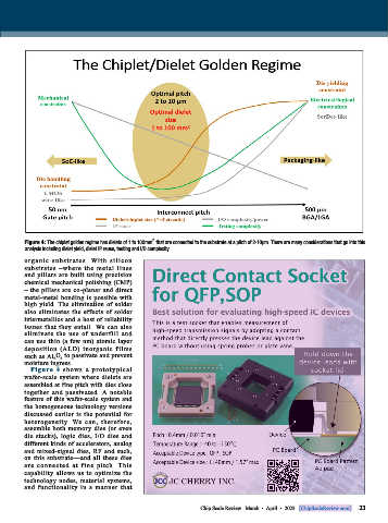
        Figure 4: The chiplet golden regime has dielets of 1 to 100mm  that are connected to the substrate at a pitch of 2-10μm. There are many considerations that go into this
        analysis including dielet yield, dielet IP reuse, testing and I/O complexity.
        organ ic subst rates. With silicon
        substrates –where the metal lines
        and pillars are built using precision
        chemical mechanical polishing (CMP)
        – the pillars are co-planar and direct
        metal-metal bonding is possible with
        high yield. The elimination of solder
        also eliminates the effects of solder
        intermetallics and a host of reliability
        issues that they entail. We can also
        eliminate the use of underfill and
        can use thin (a few nm) atomic layer
        deposition (ALD) inorganic films
        such as Al 2 O 3  to passivate and prevent
        moisture ingress.
          Figure  4  shows  a  protot y pical
        wafer-scale system where dielets are
        assembled at fine pitch with dies close
        together and passivated. A notable
        feature of this wafer-scale system and
        the homogeneous technology versions
        discussed earlier is the potential for
        heterogeneity. We can, therefore,
        assemble both memory dies (or even
        die stacks), logic dies, I/O dies and
        different kinds of accelerators, analog
        and mixed-signal dies, RF and such,
        on this substrate—and all these dies
        are connected at f ine pitch. This
        capability allows us to optimize the
        technology nodes, material systems,
        and functionality in a manner that


                                                                                                             23
                                                             Chip Scale Review   March  •  April  •  2023   [ChipScaleReview.com]  23

