Page 30 - Chip Scale Review_March April_2023-digital
P. 30
Hybrid bonding bridge for chiplet design and


        heterogeneous integration packaging

        By John H. Lau  [Unimicron Technology Corporation]

        T        he most important advantages


                 o f c h i p l e t  d e s i g n a n d
                 heterogeneous integration
        packaging, such as chip partition (driven
        by cost and technology optimization)
        and chip split (driven by  cost  and
        semiconductor manufacturing yield) are
        cost, cost, and cost [1-6]. Unfortunately, the
        most important disadvantages of chiplet
        design and heterogeneous integration
        packaging are the increase in the size of
        the package and the complexity of the
        package structure—both of which lead to
        higher packaging cost.  The higher cost is
        because of the additional package area and
        the amount of packaging effort to design
        and manufacture the interfaces (so-called
        bridges) between those chiplets, which are
        the focus of this brief article.
          An important consortium concerned
        with bridge technology is the Universal
                                ®
        Chiplet Interconnect Express  (UCIe ).
                                       ®
                                                     ®
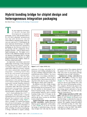
        According to the consortium’s website, the   Figure 1: UCIe   bridges. SOURCE: IEEE
        organization addresses customer requests
        for a more customizable, package-level   substrate; 2) bridge embedded in Si-  packaging method. The company obtained
        integration—combining best-in-class   interposer; and 3) bridge embedded in fan-  the patent (US 10,651,126) on May 12,
        die-to-die interconnect and protocol   out epoxy molding compound (EMC) with   2020. This is the very first patent of bridge
        connections from an interoperable,   redistribution layers (RDLs). The focus   embedded in fan-out EMC with RDLs.
        multi-vendor ecosystem. This new open   of this article is on bridges embedded in   Unimicron’s bridge embedded in
        industry standard establishes a universal   fan-out EMC with RDLs.  There are three   EMC with RDLs. Unimicron filed
        interconnect at the package level. The   different kinds of fan-out processes [8]: 1)   its patent application on May 7, 2021
            ®
        UCIe  board of directors and leadership   chip-first with chip face-up; 2) chip-first   (Figure 3). This bridge is embedded
        (promoters) include founding members   with chip face-down; and 3) chip-last.  using the fan-out chip (bridge) first with
        ASE, AMD, Arm, Google Cloud, Intel   In addition to the three bridge designs   chip face-down [10] packaging method.
        Corporation, Meta, Microsoft Corporation,   noted above, a new kind of bridge with   The company obtained the patent (US
        Qualcomm  Incorporated,  Samsung   hybrid bonding has been proposed. There   11.410,933) on August 9, 2022. This is the
        Electronics, and TSMC, along with newly-  are two options in this proposal: 1) a   first bridge patent embedded in fan-out
        elected members, Alibaba and NVIDIA.  hybrid bonding bridge with C4 bumps   EMC with RDLs the chip-first with the
                                     ®
          In [7], Intel published the UCIe  1.0   on the package substrate, and 2) a hybrid   chip face-down process.
        specification, which provides a complete   bonding bridge with C4 bumps on the   IME’s bridge embedded in EMC with
        standardized die-to-die interconnect with   chiplet wafer. The various examples   RDLs. IME filed its patent application on
        physical layer, protocol stack, software   noted in the above section are described   March 17, 2017 (Figure 4). It can be seen
        model, and compliance testing. Figure 1   in more detail below.       that this bridge is embedded by using the
        shows examples of standard packaging   Applied Materials’ bridge embedded   fan-out chip (bridge) last [11] packaging
        and advanced packaging with chiplet   in EMC with RDLs. Applied Materials   method. The company obtained the patent
        design and heterogeneous integration. It   filed its patent application on December   (US 11,018,080) on May 25, 2021. This
        can be seen that there are three different   8, 2017 (Figure 2). It can be seen that   is the very first patent using a bridge
        kinds of bridges for advanced packaging:   the bridge is embedded using a fan-out   embedded in fan-out EMC with RDLs
        1) bridge embedded in organic package   chip (bridge) first with chip face-up [9]   with chip-last or RDL-first process.

        28
        28   Chip Scale Review   March  •  April  •  2023   [ChipScaleReview.com]

