Page 31 - Chip Scale Review_March April_2023-digital
P. 31
Papers published regarding bridge
                                                                              embedded in EMC with RDLs. Since
                                                                              the developments noted above, there
                                                                              have been many papers published by
                                                                              companies such as TSMC (local silicon
                                                                              interconnect) [12], ASE (Si bridge fan-
                                                                              out chip-on-substrate) [13],  Amkor
                                                                              (S-Connect fan-out interposer) [14], SPIL
                                                                              (fan-out embedded bridge) [15], and IME
                                                                              (embedded fine interconnect) [16] in
                                                                              bridge embedded in EMC with RDLs.


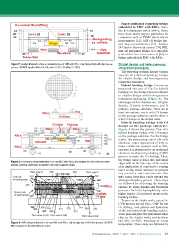
        Figure 2: Applied Materials’ bridge embedded in fan-out EMC with RDLs: chip (bridge) first with chip face-up   Chiplet design and heterogeneous
        process. SOURCE: Applied Materials, US patent 10,651,126 (May 12, 2020)  integration packaging
                                                                                The following sections discuss various
                                                                              aspects of a hybrid bonding bridge
                                                                              for chiplet design and heterogeneous
                                                                              integration packaging.
                                                                                Hybrid bonding bridge. Unimicron
                                                                              proposed the use of Cu-Cu hybrid
                                                                              bonding for the bridge between chiplets
                                                                              in chiplet design and heterogeneous
                                                                              integration packaging, (Figure 5). The
                                                                              advantages of this structure are: 1) higher
                                                                              density, 2) better performance, and 3)
                                                                              ordinary package substrate. There are at
                                                                              least two options: one is with C4 bumps
                                                                              on the package substrate, and the other is
                                                                              with C4 bumps on the chiplet wafer.
                                                                                Hybrid bonding bridge with C4
                                                                              bumps on the package substrate.
                                                                              Figure 6 shows the process flow of a
                                                                              hybrid bonding bridge with C4 bumps
                                                                              on the package substrate. For the bridge
                                                                              wafer, the processing starts off with
                                                                              chemical vapor deposition (CVD) to
                                                                              make a dielectric material such as SiO 2
                                                                              and then it is planarized by an optimized
                                                                              chemical mechanical polishing (CMP)
                                                                              process to make the Cu dishing. Then,
                                                                              the bridge wafer is diced into individual
        Figure 3: Unimicron’s bridge embedded in fan-out EMC with RDLs: chip (bridge) first with chip face-down   chips (still on the blue tape of the wafer)
        process. SOURCE: Unimicron, US patent 11,410,933 (August 9, 2022)
                                                                              after application of a protective coating
                                                                              layer on the wafer surfaces to prevent
                                                                              any particles and contaminants that
                                                                              may cause interface voids during the
                                                                              subsequent bonding process.  These steps
                                                                              are followed by activating the bonding
                                                                              surface by using plasma and hydration
                                                                              processes for better hydrophilicity and a
                                                                              higher density of a hydroxyl group on the
                                                                              bonding surface.
                                                                                To process the chiplet wafer, repeat the
                                                                              CVD process for the SiO 2 , CMP for the
                                                                              Cu dishing, and plasma and hydration
                                                                              of the activation of the bonding surface.
                                                                              Then, pick and place the individual bridge
                                                                              chip on the chiplet wafer and perform
                                                                              the SiO 2 -to-SiO 2  bonding at room
        Figure 4: IME’s bridge embedded in fan-out EMC with RDLs: chip (bridge) last or RDL-first process. SOURCE:   temperature. These steps are followed by
        IME, US patent 11,018,080 (May 25, 2021)

                                                                                                             29
                                                             Chip Scale Review   March  •  April  •  2023   [ChipScaleReview.com]  29

