Page 35 - Chip Scale Review_March April_2023-digital
P. 35
Electrical design challenges of multi-layered fan-out


        RDL MCM packaging

        By Teny Shih, Sam Lin, Andrew Kang, Yu-Po Wang  [Siliconware Precision Industries Co., Ltd.]

        H          i s t or i c a l l y,  M o or e ’s   be connected and integrated into a single   the  stacking  method  to  transform


                   Law has meant that the
                                                                              processor structure into one that is
                   semiconductor industry was   package. This scheme not only reduces   the  traditional  planar  development
                                           the bottleneck of data transmission, but
        able to maintain a cadence of next-node   also improves the operating efficiency, so   three-dimensional. By integrating and
        transistor development for processors   that the performance of the processor is   stacking smaller chips with functions
        roughly every two years. However, in   greatly improved.              such as storage, graphics, and power
        going from the 5nm node down to the   With the advent of the era of big   management, these chips can then be
        2nm node, it has become more and   data, artificial intelligence (AI), and   connected by technology to improve
        more difficult to overcome the technical   the Internet of Things (IoT), high-  performance and reach the goal either
        challenges to maintain that cadence. To   end process  chips require features   maintaining or enlarging the chip area.
        maintain the momentum of improvement   such as high-performance, low-power   Recently, the world’s major chip
        in processor performance, small chip-  consumption, and multi-functionalities.   manufacturers have been cooperating
        stacking technology has become one of   With the increase of functions, the chip   to define industry standards for chiplet
        the solutions. At a 2021 presentation by   area is also getting larger and larger.   technology. Companies participating in
        ASML, it was pointed out that further   To reduce the chip cost, advanced   the plan include ASE, SPIL, AMD, Arm,
        transistor development will encounter   packaging technology is indispensable.   Intel, Qualcomm, Samsung Electronics
        bottlenecks sooner or later in terms of   The difficulty is that in the process   and TSMC. The new industrial standard
        the performance and area of the chip—to   of introducing advanced packaging   has been named Universal Chiplet
                                                                                                       ®
        overcome these challenges  will require a   technology, it is likely that the cost will   Interconnect Express (UCIe ), which
        stacked architecture.              be increased due to unstable yield rate.   will be a standard that could bring a
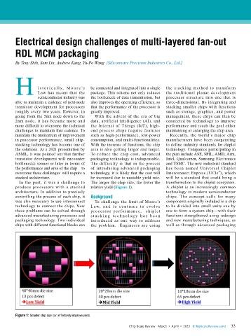
          In  the  past,  it  was  a  challenge to   The larger the chip size, the lower the   transformation to the chiplet ecosystem.
        produce processors with a stacked   relative yield (Figure 1).        A chiplet is an increasingly common
        architecture. In addition to precisely                                technology in modern semiconductor
        controlling the process of each chip, it   Background                 chips. The concept calls for many
        was also necessary to use interconnect   To challenge the limit of Moore’s   components originally included in a chip
        technology to connect the chips. Now   L aw, a nd t o c ont i nue t o evolve   to be divided into small units one by
        these problems can be solved through   processor per for ma nce,  ch iplet   one to form a system chip—with their
        advanced manufacturing processes and   s t a c k i n g t e c h n o l o g y h a s b e e n   functions strengthened using redesign
        packaging technology. Two individual   introduced as one way to address   and new manufacturing techniques, as
        chips with different functional blocks can   the problem.  Engineers are using   well as through advanced packaging


        Figure 1: Smaller chip size can effectively improve yield.

                                                                                                             33
                                                             Chip Scale Review   March  •  April  •  2023   [ChipScaleReview.com]  33

