Page 39 - Chip Scale Review_March April_2023-digital
P. 39
requires an eye mask with a width of
        0.7UI (i.e., UI=unit interval, a unit of the
        eye diagram) and a height of 0.3VDDQ ~
        0.7VDDQ (VDDQ = the supply voltage
        to the output buffers of a memory chip).
        The length of the simulated bus in this
        paper study is around 4mm.
          FO-MCM uses an organic interposer.
        The key  components in FO-MCM
        include the RDL and through-silicon
        via (TSV)-less vertical interconnects.
        The organic interposer, including a
        good eye diagram and low insertion
        loss performance of multiple RDLs with
        a coplanar GSGSG isolation scheme,
        was demonstrated. RDL lines with a
        minimum linewidth/spacing of 2/2μm
        exhibit excellent robustness, ensuring
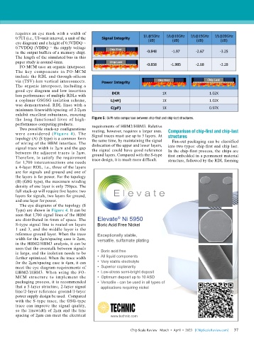
        the long functional lives of high-  Figure 5: SI/PI ratio comparison between chip-first and chip-last structures.
        performance computing products.    requirements of HBM2/HBM3. Relative
          Two possible stack-up configurations   routing, however, requires a larger area.
        were considered (Figure 4). The    Signal traces must use up to 3 layers. At   Comparison of chip-first and chip-last
        topology (A) (S type) is a common form   the same time, by maintaining the signal   structures
        of wiring of the HBM interface. The   dislocation of the upper and lower layers,   Fan-out packaging can be classified
        signal trace width is 2µm and the gap   the signal could have good reference   into two types: chip first and chip last.
        between the adjacent traces is 2µm.   ground layers. Compared with the S-type   In the chip-first process, the chips are
        Therefore, to satisfy the requirement   trace design, it is much more difficult.  first embedded in a permanent material
        for 1,700 interconnections one needs                                  structure, followed by the RDL forming
        a 4-layer RDL, i.e., three of the layers
        are for signals and ground and one of
        the layers is for power. For the topology
        (B) (GSG type), the maximum winding
        density of one layer is only 750pcs. The
        full stack-up will require five layers: two
        layers for signals, two layers for ground,
        and one layer for power.
          The eye diagrams of the topology (S
        Type) are shown in Figure 4. It can be
        seen that 1,700 signal lines of the HBM
                                                       ®
        are distributed in 6mm of space. The   Elevate  Ni 5950
        S-type signal line is routed on layers   Boric Acid Free Nickel
        1 and 3, and the middle layer is the
        reference ground layer. When the trace   Exceptionally stable,
        width for the 2µm/spacing case is 2µm,   versatile, sulfamate plating
        in the HBM2/HBM3 analysis, it can be
        seen that the crosstalk between signals
        is large, and the isolation needs to be   •  Boric acid free
        further optimized. When the trace width   •  All liquid components
        for the 2µm/spacing case is 4µm, it can   •  Very stable electrolyte
        meet the eye diagram requirements of   •  Superior coplanarity
        HBM2/HBM3. When using the FO-         •  Low-stress semi-bright deposit
        MCM str ucture to implement the       •  Optimum deposit up to 10 ASD
        packaging process, it is recommended   •  Versatile - can be used in all types of
        that a 5-layer structure, 2-layer signal      applications requiring nickel
        line/2-layer reference ground/1-layer
        power supply design be used.  Compared
        with the S-type trace, the GSG-type
        trace can improve the signal quality,
        so the linewidth of 2µm and the line
        spacing of 2µm can meet the electrical      www.technic.com


                                                                                                  2/23/2022   3:16:50 PM
                                              Chip Scale Review - Elevate Ni 5959v2.indd   1      2/23/2022   3:16:50 PM
                                              Chip Scale Review - Elevate Ni 5959v2.indd   1
                                                                                                             37
                                                             Chip Scale Review   March  •  April  •  2023   [ChipScaleReview.com]  37

