Page 36 - Chip Scale Review_March April_2023-digital
P. 36
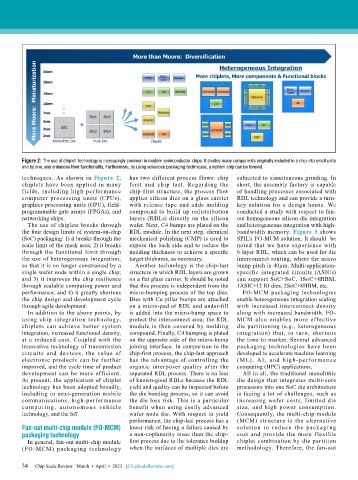
Figure 2: The use of chiplet  technology is increasingly common in modern semiconductor chips. It divides many components originally included in a chip into small units
        one by one, and enhances their functionality. Furthermore, by using advanced packaging techniques, a system chip can be formed.
        techniques. As shown in  Figure 2,   has two different process flows: chip   subjected to simultaneous grinding. In
        chiplets have been applied in many   first  and  chip  last.  Regarding  the   short, the assembly factory is capable
        fields, including high-performance   chip-first structure, the process flow   of handling processes associated with
        computer processing units (CPUs),   applies silicon dies on a glass carrier   RDL technology and can provide a turn-
        graphics processing units (GPU), field-  with release tape and adds molding   key solution for a design house. We
        programmable gate arrays (FPGAs), and   compound to build up redistribution   conducted a study with respect to fan-
        networking chips.                  layers (RDLs) directly on the silicon   out homogeneous silicon die integration
          The use of chiplets breaks through   wafer. Next, C4 bumps are plated on the   and heterogeneous integration with high-
        the four design limits of system-on-chip   RDL module. In the next step, chemical   bandwidth memory. Figure 3 shows
        (SoC) packaging: 1) it breaks through the   mechanical polishing (CMP) is used to   SPIL’s FO-MCM solution. It should  be
        scale limit of the mask area; 2) it breaks   expose the back side and to reduce the   noted that we have experience with
        through the functional limit through   molding thickness to achieve a specific   6-layer RDL, which can be used for die
        the use of heterogeneous integration,   target thickness, as necessary.  interconnect routing, where the micro
        so that it is no longer constrained by a   Another technology is the chip-last   bump pitch is 40µm. Multi-application-
        single wafer node within a single chip;   structure in which RDL layers are grown   specific integrated circuits (ASICs)
        and 3) it improves the chip resilience   on a flat glass carrier. It should be noted   can support SoC+SoC, 1SoC+4HBM,
        through scalable computing power and   that this process is independent from the   1ASIC+12 IO dies, 2SoC+8HBM, etc.
        performance; and 4) it greatly shortens   micro-bumping process of the top dies.   FO-MCM packaging technologies
        the chip design and development cycle   Dies with Cu pillar bumps are attached   enable heterogeneous integration scaling
        through agile development.         on a micro-pad of RDL and under-fill   with increased interconnect density
          In addition to the above points, by   is added into the micro-bump space to   along with increased bandwidth. FO-
        using chip integration technology,   protect the interconnect area; the RDL   MCM also enables more effective
        chiplets can achieve better system   module is then covered by molding   die partitioning (e.g., heterogeneous
        integration, increased functional density,   compound. Finally, C4 bumping is plated   integration) that, in turn, shortens
        at a reduced cost. Coupled with the   on the opposite side of the micro-bump   the time to market. Several advanced
        innovative technology of transmission   joining interface. In comparison to the   packaging technologies  have  been
        circuits and devices, the value of   chip-first process, the chip-last approach   developed to accelerate machine learning
        electronic products can be further   has the advantage of controlling the   (ML), AI, and high-perfor mance
        improved, and the cycle time of product   organic interposer quality after the   computing (HPC) applications.
        development  can  be  more  efficient.   separated RDL process. There is no loss   All in all, the traditional monolithic
        At present, the application of chiplet   of known-good RDLs because the RDL   die design that integrates multi-core
        technology has been adopted broadly,   yield and quality can be inspected before   processors into one SoC die architecture
        including in next-generation mobile   the die bonding process, so it can avoid   is facing a lot of challenges, such as
        communications, high-performance   the die loss risk. This is a particular   increasing wafer costs, limited die
        c omput i ng, aut onomou s veh icle   benefit when using costly advanced   size, and high power consumption.
        technology, and the IoT.           wafer node die. With respect to yield   Consequently, the multi-chip module
                                           performance, the chip-last process has a   (MCM) structure is the alternative
        Fan-out multi-chip module (FO-MCM)   lower risk of having a failure caused by   solution to reduce the packaging
        packaging technology               a non-coplanarity issue than the chip-  cost and provide the more f lexible
          In general, fan-out multi-chip module   first process due to the tolerance buildup   chiplet combination by die partition
        (FO-MCM) packaging technology      when the surfaces of multiple dies are   methodology. Therefore, the fan-out

        34   Chip Scale Review   March  •  April  •  2023   [ChipScaleReview.com]
        34

