Page 32 - Chip Scale Review_March April_2023-digital
P. 32

annealing to achieve covalent bonding
                                                                              between  oxide  layers  and  metallic
                                                                              bonding between Cu-Cu contacts and the
                                                                              diffusion of Cu atoms.
                                                                                For the package substrate, the process
                                                                              is to stencil print the solder paste on the
                                                                              substrate and then reflow into C4 solder
                                                                              bumps. For the final assembly, the bridge
                                                                              + chiplets module is picked and placed on
                                                                              the package substrate, then  the C4 bumps
                                                                              are reflowed.
                                                                                Hybrid bonding bridge with C4
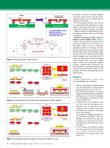
                                                                              bumps on the chiplet wafer. Figure
                                                                              7 shows the process flow of the hybrid
                                                                              bonding bridge with C4 bumps on
                                                                              the chiplet wafer. It can be seen that,
                                                                              compared with the C4 bumps for the
                                                                              package substrate case, the process steps
                                                                              for the bridge wafer and the chiplet wafer
                                                                              are the same up to the bridge-to-chiplet
                                                                              wafer bonding step. After that, the C4
                                                                              bumps are fabricated by wafer bumping
        Figure 5: Hybrid bonding bridge. SOURCE: Unimicron                    on the chiplet wafer. Then, the chiplet
                                                                              wafer is diced into individual modules
                                                                              (bridge + chiplets with C4 bumps). The
                                                                              final assembly is accomplished by picking
                                                                              and placing the individual module on the
                                                                              package substrate and reflowing the C4
                                                                              solder bumps.

                                                                              Summary
                                                                                S o m e  i m p o r t a n t  r e s u l t s  a n d
                                                                              recommendations are as follows:

                                                                                •  The key advantages of chiplet design
                                                                                  and heterogeneous integration
                                                                                  packaging are cost, cost, and cost.
                                                                                •  The key disadvantages of chiplet
                                                                                  design and heterogeneous integration
                                                                                  packaging are to increase package
                                                                                  size and package complexity, which
        Figure 6: Hybrid bonding bridge with C4 bumps on the package substrate. SOURCE: Unimicron  leads to higher cost.
                                                                                •  In general, the semiconductor cost
                                                                                  is a few times the packaging cost,
                                                                                  therefore, the  savings that can be
                                                                                  achieved with chiplet design and
                                                                                  heterogeneous integration packaging
                                                                                  are worth pursuing.
                                                                                •  The patents for bridges embedded in
                                                                                  fan-out EMC with RDLs with chip
                                                                                  (bridge) first and chip face-up, chip
                                                                                  (bridge) first and chip face-down,
                                                                                  and chip-last or RDL-first, have been
                                                                                  provided.
                                                                                •  A new bridge with hybrid bonding
                                                                                  has been proposed. Its advantages
                                                                                  a r e : h i g h e r d e n s i t y, b e t t e r
                                                                                  performance, less process steps, and
                                                                                  lower cost.
        Figure 7: Hybrid bonding bridge with C4 bumps on the chiplet wafer. SOURCE: Unimicron

        30   Chip Scale Review   March  •  April  •  2023   [ChipScaleReview.com]
        30
   27   28   29   30   31   32   33   34   35   36   37