Page 43 - Chip Scale Review_March April_2023-digital
P. 43
Wafer-scale integration for graphene-based


        optoelectronics, sensors, and imaging devices

        By Souvik Ghosh [imec vzw], Amaia Zurutuza  [Graphenea], Alice Guerrero  [Brewer Science]

        T        he dawn of the 21  century   be obtained via electrochemical spalling   surface because of its low C solubility,


                                 st
                 kick-started an era of two-
                 dimensional (2D) materials,   of graphitic membranes in solution. Both   facilitating monolayer, and even bilayer
                                           techniques facilitate easy and selective access
                                                                              graphene growth control.
        with graphene in the forefront. Graphene   to surface and edges of the nanosheets,   Additionally, research is ongoing to
        is the most well-known 2D material   thereby promoting nanodecoration   enable graphene growth on rigid template
        and is often being referred to as the   and targeted functionalization of these   wafers. If Cu is sputtered directly on Si/
        “wonder material.” The exceptional   nanosheets. Despite being a robust technique   SiO 2  wafers followed by graphene growth,
        properties of graphene, such as very high   to manufacture graphene sheets, mechanical   the resultant SLG quality is relatively
        carrier mobilities and ballistic transport,   and electrochemical exfoliations remain   poor due to the polycrystalline nature
        promise a host of applications that range   a challenging approach to enable fab   and small grain structure of the Cu layer
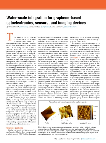
        from sensors, optical modulators, and   integration. The inherently small size of   (see Figure 1). Metal epitaxy on template
        detectors to rapid-scan imagers, thermal   graphene flakes and the lack of control over   wafers such as sapphire can provide a
        management, and even room-temperature   the number of layers during graphene flake   single catalyst orientation and ideally a
        graphene-based spintronic devices. An   synthesis make it very difficult to position   single-crystalline SLG is grown. In this
        interesting property of graphene is its   these flakes accurately on a target wafer.  respect, epitaxial graphene growth has
        linear energy-momentum dispersion that   The most promising graphene growth   been demonstrated on epitaxial Cu(111)/
        enables light absorption from the ultraviolet   route is via chemical vapor deposition (CVD).   sapphire(0001) wafers, but also other wafer
        to the terahertz regime. This extreme   In fact, soon after Geim and Novoselov’s   types like Ge(110) can be used for epitaxial
        broadband capability is a unique material   mechanical exfoliation method, CVD quickly   graphene growth. The latter one is not
        property and makes it very interesting for   caught up to enable large-scale controlled   straightforward because the process window
        on-chip optical communication because   SLG synthesis. There are numerous catalyst   to grow high-quality graphene is rather small
        information can be multiplexed over a   substrates available that enable high-quality   but avoids transition metal contamination
        wider range of wavelengths and enable   graphene growth. These substrates include   issues during graphene integration.
        ultrafast communication.           transition metal foils such as Cu, Ni, Fe, Pt,   Graphene growth on a thin epitaxial Ge layer
          The most high-end graphene-based   and even alloys. Cu or alloys like CuNi are   is also very complicated because of diffusion
        applications (i.e., optical I/O devices), though   interesting due to their favorable catalytic   of Si into the Ge layer, which increases the
        in active development at laboratory scale,   properties, low C solubility and relatively   roughness of the Ge layer. Nevertheless,
        will need at least another decade to come   low cost. The governing graphene growth   because SLG growth on epitaxial surfaces
        to the market simply due to limitations of   mechanism relies on dissolution of the C   can follow a preferred orientation, this
        scalability, yield, and performance metrics   species and subsequent saturation of the   growth route is expected to give the highest
        [1]. In the near term, single-layer-graphene   surface. Cu remains an interesting catalyst   graphene quality due to the absence of grain
        (SLG) is already seeing an increase in
        market opportunities mainly in the field
        of (low-cost) sensors. These applications
        will be enabled by the development of new
        graphene growth and transfer techniques.
        This article summarizes the near and
        long-term outlook using the practical
        benefits of graphene in view of its time-to-
        market. Further, the specific technological
        support structure needed to consider the
        material as a viable option to be compatible
        with existing semiconductor fabrication
        infrastructure will also be outlined.

        Graphene synthesis                 Figure 1: Atomic force microscopy inspection after graphene growth on a Cu foil, a Si/SiO 2 /Cu wafer and
          Graphene synthesis was first achieved via   a sapphire/Cu wafer. Clear topography variations are present after graphene growth on a Cu foil, but the
        mechanical exfoliation from highly-oriented   observed grain size is much larger compared to a graphene growth on a Si/SiO 2 /Cu wafer (the scan size of both
                                           AFM images is 10μm). A strongly reduced surface roughness can be obtained when graphene is grown on an
        pyrolytic graphite (HOPG) [2] and can also   epitaxial template wafer (e.g., Cu(111)/sapphire(0001)).
                                                                                                             41
                                                             Chip Scale Review   March  •  April  •  2023   [ChipScaleReview.com]  41

