Page 45 - Chip Scale Review_March April_2023-digital
P. 45
plasma clean. A protection layer on top of
                                                                              graphene could also be envisioned to avoid
                                                                              direct graphene/TBM contact.
                                                                              Summary
                                                                                To achieve a reliable transfer process
                                                                              and to maintain the intrinsic properties
                                                                              of graphene, it is known that device
                                                                              performance can improve when SLG
                                                                              is transferred on smooth target wafers.
                                                                              To avoid high surface roughness when
                                                                              integrating graphene in the BEOL (e.g., on
                                                                              a readout integrated circuit [ROIC] wafer),
                                                                              a planarization step of the top dielectric will
                                                                              have to be implemented before graphene
                                                                              transfer. After transferring graphene on
                                                                              such a wafer, it will have to be capped with
                                                                              a dielectric followed by graphene patterning
                                                                              and contact fabrication. Following this
                                                                              approach, a BEOL operational graphene
                                                                              transistor can be achieved that can serve a
                                                                              multitude of applications [3].
                                                                              Acknowledgments
                                                                                This work is supported by the imec
                                                                              IIAP optical I/O program and received
                                                                              funding  from  the  European  Union’s
                                                                              Graphene Flagship grant agreement CORE
                                                                              3 (No 881603) and 2D-EPL (No. 952792).
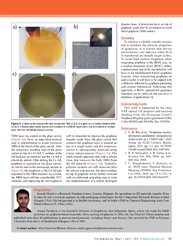
        Figure 3: a) Glass carrier system with laser release and TBM; b) SLG on a glass carrier system obtained after
        Cu etch; c) Bonded glass carrier system with graphene on a 200mm target wafer; and d) Graphene on a target
        wafer after the full 200mm transfer process.                          References
                                                                                 1.  C. H. Wu, et al., “Graphene electro-
        TBM layer are coated on the glass carrier    will be important to improve the graphene   absorption modulators integrated at
        (Figure 3a). Next, an edge bead removal   transfer result. Next, the glass carrier that   wafer-scale in a CMOS fab,” 2021
        step is implemented to avoid excessive   contains the graphene layer is bonded on   Symp. on VLSI Circuits, Kyoto,
        TBM at the bevel of the glass carrier. After   top of a target wafer and the temporary   Japan, 2021, pp. 1-2, doi: 10.23919/
        the temporary bonding step of the glass   carrier is subsequently removed using   VLSICircuits52068.2021.9492495.
        carrier on top of a Cu foil, C residues at the   a laser release process (Figure 3c). The   2.  K. S. Novoselov, A. K. Geim, et al.,
        foil backside are removed and the Cu foil is   whole transfer approach ends with a solvent   Science Vol. 306, 5696, pp. 666-
        selectively etched. After etching the Cu foil,   clean that removes the bulk TBM from   669, Oct. 2004.
        graphene is exposed on the glass carrier.   the 2D material (Figure 3d). Typically,   3.  C. Huyghebaert, T. Scharm, et
        As can be seen in the microscopy picture in   polymer residues are still observed after   al., IEEE Inter. Electron Devices
        Figure 3b, the roughness of the Cu foil gets   the solvent strip process, but these residues   Meeting (IEDM), San Francisco,
        imprinted in the TBM material. As a result,   on top of graphene can be further removed   CA, USA, 2018, pp. 22.1.1-22.1.4,
        the TBM layer still has considerable TTV   with an additional annealing step or even   doi: 10.1109/IEDM.2018.8614679.
        variation, and improving the foil roughness   the implementation of a remote hydrogen


                       Biographies
                         Souvik Ghosh is a Research Scientist at imec, Leuven, Belgium. He specializes in 2D materials transfer. Prior
                       to imec he was a research engineer on chip packaging technologies for the Components Research division at Intel
                       (Oregon, USA). His background is in flexible electronics, and he holds a PhD in Chemical Engineering from Case
                       Western Reserve U. (Ohio, USA).

                         Amaia Zurutuza is the Scientific Director of Graphenea, San Sebastian, Spain, where she leads the R&D
                       activities on graphene-based materials. Since joining Graphenea in 2010, she has filed for fifteen patents and
          published more than 85 publications in peer-reviewed journals, including Nature and Science. She received her PhD in Polymer
          Chemistry from the U. of Strathclyde (Glasgow, UK) in 2002.

            Contact author: Alice Guerrero/Brewer Science; email aguerrero@brewerscience.com


                                                                                                             43
                                                             Chip Scale Review   March  •  April  •  2023   [ChipScaleReview.com]  43

