Page 44 - Chip Scale Review_March April_2023-digital
P. 44
boundaries and its low surface roughness.   adoption and hesitation aside, existing   polymer has been applied in a successful
        A thermal decomposition route can also   layer transfer technology has already   and reproducible manner. It is imperative
        produce high-quality graphene on SiC,   been demonstrated to enable new device   that alternate TBMs be identified to enable
        but is often considered to be less scalable   possibilities. Furthermore, a layer transfer   quality-controlled 2D transfer that meets
        compared to CVD, due to the need of large –   can potentially bring an epitaxial 2D layer   industrial-scale requirements because
        and as a result – expensive SiC wafers.  on an amorphous dielectric surface that   uniform bonding of a temporary carrier
          Nowadays, CVD synthesis of SLG is   is otherwise impossible to achieve via    system with a PMMA layer will be very
        mostly done on Cu foils at a manufacturing   direct growth.           difficult to achieve in a reproducible
        scale. However, SLG grown on Cu foils   The transfer of graphene from a growth   manner. Furthermore, such TBMs will need
        typically has high topography variations   substrate to a target device wafer typically   to be specifically selected to be compatible
        over a macroscopic scale because of the   requires an intermediate carrier to support   with a release process (e.g., laser debond
        flexible nature of the foils and the high   fragile 2D materials. As often reported in   approach). To enable this laser release
        graphene growth temperature (typically   literature, R&D-scale transfer approaches   mechanism, the TBM can be complemented
        well above 800°C). This foil roughness can   use poly-(methyl methacrylate) (PMMA) as   with a second layer that specifically is
        likely be further improved by incorporating   a support layer. This is generally perceived   compliant with the release mechanism (e.g.,
        electropolishing and annealing before   as the golden standard aiding in transfer   laser-absorbent materials). Finally, the last
        the actual graphene growth process.   of 2D flakes and even CVD materials.   key element governing the selection of an
        However, because of the polycrystalline   Here, PMMA is dissolved in a solvent (e.g.,   appropriate TBM is its adhesion with the
        nature of the foils themselves it will be   anisole), spin-coated on the 2D material,   graphene layer and that with the carrier
        difficult to completely avoid graphene grain   and possibly adhered to a thermal release   system. The adhesion between the TBM and
        boundaries. Nevertheless, high graphene   tape (TRT). Next, graphene is released from   the 2D of interest needs to be high enough
        mobilities have been reported for CVD   its growth substrate via Cu etching or even   such that during mechanical, chemical, or
        graphene grown on Cu foil, which could   intercalation-based (i.e., electrochemical)   electrochemically assisted debonding, the
        make this technique ideally suited for   release methods. The released graphene   2D is spalled or discharged from the growth
        several graphene-based sensor applications.   layer is then laminated or bonded to a target   substrate while keeping the TBM-2D
        To enable high-end graphene applications, a   wafer. Finally, the adhesive is stripped   interface intact.
        controlled and oriented growth on epitaxial   to expose the 2D material. While a TRT-
        catalyst template wafers is likely needed.    based transfer method is viable for proof-  A manufacturable graphene
        However, this growth approach complicates   of-concept device demonstration, it remains   transfer route from Cu foil
        transfer because a lateral wet-chemical   challenging to implement this process in a   The highest quality graphene is grown
        etch-based transfer is more difficult to   production environment. Further, manual   on epitaxial template wafers, but debonding
        implement and recycling of the growth   bonding and debonding steps introduce   large-scale graphene from these wafers
        wafer is preferred from a cost perspective.  user-level variance that manifest in the form   has not yet been demonstrated in a fab
                                           of wrinkles, surface-potential variation,   environment. Because graphene quality
        Layer transfer technologies        and macroscopic cracks. A viable and   is sufficient for several applications when
        applicable to 2D materials         scaled industrial approach to demonstrate   it is grown on a Cu foil, and the graphene
          Because the most mature graphene   transfer of graphene on 200mm, or even   release can be easily achieved via etching
        growth technique is CVD on a transition   300mm target wafers, likely requires the   processes, it is likely that this foil approach
        metal template, most graphene applications   use of a rigid substrate as a temporary   combined with an etch-based release step
        require the development of a layer transfer   carrier instead of TRT. A rigid carrier   is the preferred choice for introducing
        technology. Such a technology, especially   will prevent nonuniform and excessive   graphene in the BEOL. To achieve a reliable
        for front-end-of-line (FEOL) applications,   expansion typically observed for TRT-based   transfer, the use of a rigid temporary
        is the “new kid on the block.” It is untested   transfers. Furthermore, a rigid temporary   glass carrier is an option as it optimizes
        and historically unqualified to compete   carrier is compatible with existing 200mm   the bonding step to the target wafer and
        with mainstream fab integration processes   and 300mm (de)bonding and cleaning   facilitates the etching and cleaning steps.
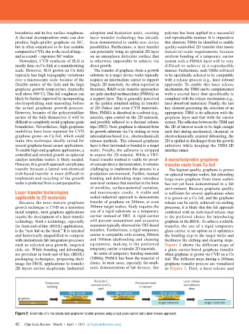
        such as selected-area growth, targeted   equipment, making it the preferred   Figure 2 shows the different steps of
        etch, etc. While bonding and debonding   temporary carrier to transfer 2D materials.  a glass carrier-based graphene transfer
        are prevalent in back-end-of-line (BEOL)   In terms of temporary bonding materials   when graphene is grown via CVD on a Cu
        packaging techniques, proposing their   (TBMs), PMMA has been the material of   foil. The different steps during a 200mm
        usage for FEOL applications to transfer   choice. In most cases, especially for small-  graphene transfer process are visualized
        2D layers invites skepticism. Industrial   scale demonstration of lab devices, this   in Figure 3. First, a laser release and


        Figure 2: Schematic of a manufacturable graphene transfer process using a rigid glass carrier and a laser release approach.

        42   Chip Scale Review   March  •  April  •  2023   [ChipScaleReview.com]
        42

