Page 26 - Chip Scale Review_March April_2023-digital
P. 26
is not p ossible i n homoge ne ou s   captures the pitch at which the dies are   are typically this size). As the die size
                                                                                            2
        monolithic chips, no matter how big.   connected to the substrate. The right-hand   goes below 1mm , the yield approaches
        Furthermore, it is possible to scale   side is bound by the ball grid array (BGA)   100% in mature technologies (in fact, at
        these systems to wafer scale allowing   pitches on today’s PCBs (~100s of μm) and   these dimensions, we can blind-build these
        us to pack high-compute power in very   the left-hand side represents the contacted   dies and expect them to work) and so the
        small form factors. We would not be   gate pitch at which transistors on the chip   optimal die size is expected to be between
                                                                                                          2
                                                                                         2
        able to do this were it not for the fine   may be connected (~10s of nm). The y-axis   1 and 100mm . If dies go below 1mm , two
        bump and trace pitch and the close die   depends on what is being plotted.   effects begin to dominate: die handling
        placement. The fine-pitch capability   Let’s consider the die size shown in   becomes difficult (both for assembly and
        combined with the ability to place   brown. Large dies yield poorly, and as we   test), and kerf loss becomes appreciable.
        dies in close proximity, allows these   decrease the die size, the yield increases; but   Another consideration is IP reuse.
        heterogeneous systems to behave as if   below about 100mm , the yield increases—  Generally speaking, small dies have less
                                                           2
        they were monolithic. This last point   though slowly (this is why memory dies   content and are less likely to be specialized.
        is crucial and differentiates today’s
        heterogeneous systems from those of
        yore. One thing we must mention is
        that dielets, today, are assembled on
        a substrate by mechanical placement
        and this is a limitation on overlay
        tolerance  (currently  ~+/-1μm),  but
        we expect both steady improvement
        in placement accuracy and perhaps
        true lithographically-defined ways of
        connecting the dies.
          The newfound capability described
        above changes the way in which we can
        build system on chip (SoC) structures.
        Today’s SoCs are typically synthesized
        with soft intellectual property (IP)
        d e sig n blo c k s u si n g h ig h -le vel
        synthesis tools. Over 80% of these IP
        blocks have been instantiated on some
        other SoC or on test sites. However,
        every time we tape out a new SoC, we
        re-synthesize these very IP blocks in
        new configurations, reduce them to
        schematics, and finally, lay them out
        physically and re-harden them. This
        is a time-consuming and expensive
        task and contributes enormously to the
        so-called non-recurring engineering
        (NRE) of building a new chip. Bigger
        chips take longer and cost more and
        limit the number of players who can
        play this game. In 2016, I published
        a paper [1] where I suggested that we
        could pre-build a bunch of commonly
        used dielets and stock them, so that
        we could build a complex SoC by
        assembling these prefabricated dies
        usi ng these advanced packagi ng
        constructs. This vision is slowly, but
        surely, taking root.

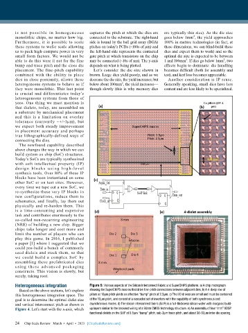
        Heterogeneous integration          Figure 5: Various aspects of the Silicon Interconnect Fabric and SuperCHIPS platform. a) A chip micrograph
          Based on the above sections, let’s explore   showing the SuperCHIPS macros that drive fine-pitch connections between adjacent dies; b) A 4-deep row of
        this heterogeneous integration space. The   pillars at 10μm pitch yields an effective “bump” pitch of 2.5μm. c) The I/O drivers are small and must be contained
        goal is to determine the optimal dielet size   at the 10μm pitch, and consist of a cascaded set of inverters with the capability of both synchronous and
        and vertical interconnect pitch as shown in   asynchronous modes. d) The silicon interconnect fabric (Si IF) is a full-thickness silicon wafer with inorganic build-
                                                                                                          2
        Figure 4. Let’s start with the x-axis, which   up layers similar to the backend wiring of a 90nm CMOS technology structure. e) An assembly of four 1mm  UDSP
                                           functional dielets on the Si IF at 9.8μm “bump” pitch, sub-2μm trace pitch, and about 30-50μm inter-die spacing.
        24   Chip Scale Review   March  •  April  •  2023   [ChipScaleReview.com]
        24

