Page 22 - Chip Scale Review_March April_2023-digital
P. 22
Heterogeneous integration and chiplets and dielets:


        why the hype?

        By Subramanian (Subu) Iyer  [The UCLA Center for Heterogeneous Integration and Performance Scaling (UCLA CHIPS),
        Samueli School of Engineering, University of California, Los Angeles]
        O          ver the last few  years,   footprint. This has fueled the well-known   The reason why we would like to


                   there has been an over-
                                           W h ile i n it ially t h is scali ng was
                                                                              penalty of off-chip communication
                   abundance of attention paid   Moore’s  “Law”  for  miniaturization.   grow die size has to do with the huge
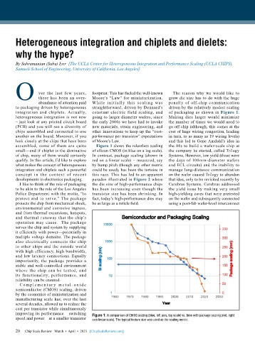
        to packaging driven by heterogeneous   straightforward, driven by Dennard’s   driven by the relatively modest scaling
        integration  and chiplets. Actually,   constant electric field scaling, and   of packaging as shown in Figure 1.
        heterogeneous integration is not new   going to larger diameter wafers, since   Making dies larger would minimize
        – just look at any printed circuit board   the early 2000s we have had to invoke   the number of times we would need to
        (PCB) and you will see a diversity of   new materials, strain engineering, and   go off chip (although, this comes at the
        chips assembled and connected to one   other innovations to keep up the “cost-  cost of huge wiring congestion, leading
        another on the board. Moreover, if you   performance per transistor” expectations   in turn, to as many as 19 wiring levels)
        look closely at the chips that have been   of Moore’s Law.            and this led to Gene Amdahl’s idea in
        assembled, some of them are quite    Figure 1 shows the relentless scaling   the 80s to build a wafer-scale chip at
        small—and if chiplet is the diminutive   of silicon CMOS (in blue on a log scale).   the company he started, called Trilogy
        of chip, many of them would certainly   In contrast, package scaling (shown in   Systems. However, low yield (those were
        qualify. In this article, I’d like to explore   red on a linear scale) – measured, say   the days of 100mm-diameter wafers
        what makes the concept of heterogeneous   by bump pitch (though any other metric   and ECL circuits) and the inability to
        integration and chiplets such a powerful   could be used), has been the tortoise in   manage long-distance communication
        concept in the context of recent   this race. This has led to an apparent   on the wafer caused Trilogy to abandon
        developments in electronics packaging.  paradox illustrated in Figure 2 where   that idea, only to be revisited recently by
          I like to think of the role of packaging   the die size of high-performance chips   Cerebras Systems. Cerebras addressed
        to be akin to the role of the Los Angeles   has been increasing even though the   the yield issue by making very small
        Police Department with the motto, “to   transistor size has been shrinking. In   high-yielding cores that were pretested
        protect and to serve.” The package   fact, today’s high-performance dies may   on the wafer and subsequently connected
        protects the chip from mechanical shock,   be as large as a reticle field.   using a post-fab wafer-level interconnect
        environmental and corrosive ingress,
        and from thermal excursions, hotspots,
        and thermal runaway that the chip’s
        operation may cause.  The package
        serves the chip and system by supplying
        it efficiently with power—potentially in
        multiple voltage domains. The package
        also electrically connects the chip
        to other chips and the outside world
        with high efficiency, high bandwidth,
        and low latency connections. Equally
        importantly, the package provides a
        stable and well-controlled environment
        where the chip can be tested, and
        its functionality, performance, and
        reliability can be ensured.
          C om p l e me n t a r y   me t a l - o x i d e
        semiconductor (CMOS) scaling, driven
        by the economics of miniaturization and
        manufacturing scale has, over the last
        several decades, allowed us to reduce the
        cost per transistor while simultaneously
        improving its performance – switching   Figure 1: A comparison of CMOS scaling (blue, left axis, log scale) vs. time with package scaling (red, right
        speed and power – at a smaller transistor   axis linear scale). The typical feature size was used as the scaling metric.


        20
        20   Chip Scale Review   March  •  April  •  2023   [ChipScaleReview.com]

