Page 18 - Chip Scale Review_March April_2023-digital
P. 18
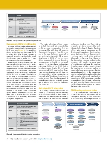
Figure 3: Direct placement D2W hybrid bonding process flow.
        Reconstructed D2W hybrid bonding     The major advantage of this process   and copper bonding pad. Two guiding
          A recent publication introduces a novel   is its full front-end fab compatibility,   principles are being explored for self-
        integration method called reconstructed   and  there  are  no  materials  that  are   aligned die bonding: 1) shaping the die to
        D2W bonding (Figure 4) that combines   incompatible with the fab present   achieve ultra-precise dimensions; and 2)
        direct and collective placement D2W   throughout the process flow. However,   defining guiding pads on the die surface
        bonding [5]. The direct placement   one of the main challenges is controlling   using hydrophilic and hydrophobic
        approach is used to mechanically attach   and optimizing the oxide fill process.   r e g i o n s  p a t t e r n e d w i t h o p t i c a l
        the dies to a carrier wafer, but it only   Analogies to FOWLP apply, where   lithography at the wafer level. However,
        provides a mechanical connection.  silicon content, die thickness, deposition   the singulation, cleaning, and activation
          Once the chiplets are formed, they are   temperatures, and oxide properties all   processes still require the same level
        permanently attached to a carrier wafer   impact the wafer shape and contact   of precision as traditional die bonding.
        with the die either facing up or down, and   pitch scalability of the W2W hybrid   The placement of dies in self-aligned
        the gap between them is filled with silicon   bonding process. Despite this challenge,   die bonding can be coarser, leading to
        oxide, which is a front-end compatible   reconstructed D2W bonding has shown   potentially lower process costs, but the
        version of fan-out wafer-level packaging   great promise in achieving full front-end   increased complexity in die preparation,
        (FOWLP) that is inorganic. The challenge   fab compatibility while maintaining the   guiding pad definition and combination
        in this step is that the oxide thickness   highest level of cleanliness throughout the   with crucial chemical mechanical
        needs to be significantly higher to support   entire process flow. Further research is   planarization (CMP) processes, must also
        the overall chiplet height, including the   needed to optimize the oxide fill process   be considered. Self-aligned die bonding
        silicon substrate and metal interconnects.   and to address other potential challenges   has high potential, but further research
        Afterward, the dies and oxide layer are   that may arise.             and development is necessary to improve
        planed thoroughly, and through-dielectric                             the integration process [6].
        interconnects and hybrid bond pads are   Self-aligned D2W integration
        created at the wafer level. The actual   Currently, research institutes are   D2W bonding equipment status
        hybrid bonding and electrical contact are   focusing on self-aligned die bonding,   The preparation and conditioning of
        done later in a W2W bonding process.   which follows similar key steps to   surfaces for direct placement fusion
        Cleanliness must be strictly maintained   traditional die bonding such as cleaning   and hybrid bonding of dies on wafers
        throughout the process.            and activation of the dielectric interface   is a critical step. Challenges related to


        Figure 4: Reconstructed D2W hybrid bonding process flow.

        16   Chip Scale Review   March  •  April  •  2023   [ChipScaleReview.com]
        16

