Page 15 - Chip Scale Review_March April_2023-digital
P. 15
Accelerating 3D and heterogeneous integration with


        high-volume D2W hybrid bonding

        By Thomas Uhrmann  [EV Group] and Nelson Fan  [ASMPT]

        T        he semiconductor industry is   top of each other in a 3D-integrated   l i n e s . T h i s p r o c e s s h a s p r ove n


                 undergoing a revolutionary
                 t ransfor mation with the   circuit (IC) configuration. In contrast,   successful for complementary metal-
                                                                              oxide semiconductor (CMOS) image
                                           the add-on scheme uses a base die as
        adoption of heterogeneous integration   one of the chiplets with little to no   sensors and various memory and logic
        and chiplet-based design, marking a   partitioning and adds another chiplet   technologies. W2W hybrid bonding
        fundamental turning point. Monolithic   (or multiple chiplets) with additional   has been mature for over a decade,
        2D scaling options often come with   features, such as extra memory. The   with equipment and process now well
        complex and costly issues and limited   add-on chiplets are stacked above or   established. It enables contact pitch of
        scaling benefits for a system. Chiplets,   below the original monolithic chiplet   less than 1µm in production, but die
        therefore, are an inevitable solution   in the 3D-IC configuration [1]. The   size and grid matching are required.
        to meet the demands of the scaling   partition scheme is focused more on   Each bonding layer consists of only one
        roadmap and performance, power,    cost and footprint savings, while the   node, and cumulative yield decreases
        area-cost and time-to-market (PPACt)   add-on method  is geared  towards   the overall stack yield for high layer
        requirements. High-perfor mance    performance and power improvement,   count. However, W2W bonding offers
        applications, including ar tif icial   s u c h a s f o r h i g h - p e r f o r m a n c e   high-throughput capabilities.
        intelligence (AI), augmented/virtual   computing applications. Cost savings   Die-to-wafer (D2W) hybrid bonding
        reality, and autonomous driving, require   are greater as the monolithic 2D die   is a relatively new technology, and
        specialized processors for each task,   area increases and wafer costs become   its process and equipment  maturity
        making chiplet integration necessary.   more expensive. In both cases, savings   are still evolving, resulting in many
        This design approach is already being   are optimized when the partitioned   challenges. The contact pitch for this
        used in various forms, from hybrid   t wo ch iplets have t he sa me si ze   bonding method is currently at 9µm
        bonding to 2.5D interposers, and is   because it improves the yield for each   in production, but this is expected
        equally critical for consumer and mobile   die individually. In addition to cost   to decrease rapidly to 2µm. One
        devices to keep up with performance   savings, partitioning is also expected to   advantage of D2W bonding is that
        and flexibility requirements.      lead to effective capacity improvement   there are no limitations on die size or
          The shift to chiplet integration,   due to higher yields in smaller chiplets.   system segmentation. Additionally,
        however, requires a complete overhaul   Technology considerations of 3D-ICs   chiplets of different nodes can be
        of the semiconductor manufacturing   and the various component flavors of   combined, providing a high level of
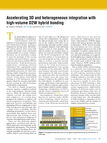
        process. While 2D transistor scaling   3D-ICs are depicted in Figure 1.  flexibility. However, binning may be
        remains relevant, the rising costs   Heterogeneous integration relies   necessary because of the varying yields
        a nd c omplex it y of scal i ng h ave   heavily on wafer-to-wafer (W2W)   of individual dies. The throughput
        prompted the industry to embrace 3D   hybr id bond i ng, wh ich i nvolves   of D2W bonding is dependent on the
        and heterogeneous integration. This   stacking and electrically connecting   size of the chiplets and the number of
        approach involves assembling and   wafers from different production   chiplets integrated into a system.
        packaging different components or dies
        with varying sizes and materials into
        a single device or package, thereby
        enhancing performance on new device
        generations that support these new
        applications and leading to more
        precise and customized mapping of
        customer and application requirements.
          There are two different chiplet
        approaches: partition and add-on.
        Which approach is used depends on the
        application and purpose. The partition
        scheme involves breaking down the
        original monolithic die into two or more
        smaller chiplets and stacking them on   Figure 1: Heterogeneous integration and connection options along different packaging levels from chip- to
                                           board-level.

                                                                                                             13
                                                             Chip Scale Review   March  •  April  •  2023   [ChipScaleReview.com]  13

