Page 11 - Chip Scale Review_March April_2023-digital
P. 11
companies typically operate in an ISO-7   the tape frame. In early 2017, we began   develop the technology for 3D stacking
        environment and require an upgrade to   developing the DBI  Ultra assembly   [11]. Additionally, Gao, et al., showed
                                                             ®
        their infrastructure for the hybrid bond   process for die-to-wafer, which was   the reliability performance of hybrid
        advanced interconnect technology. As   launched at the 2019 ECTC. This   bond interconnect test vehicles with
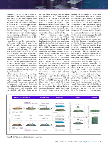
        the pitch of the interconnect continues   process is shown in  Figure 2. The   and  without  TSVs  was  en hanced
        to scale in die-to-wafer applications,   hybrid bond interconnect is formed with   compared to the microbump [12].
        the micro-environment cleanliness   a standard BEOL Cu damascene process   Given an all-Cu interconnect, there
        specifications will tighten. Cluster tool   that includes dielectric deposition, etch,   is no driving force for intermetallic
        platforms are now being considered   barrier layer, Cu seed, Cu plate and   formation or Kirkendall voids that lead
        for efficiencies of scale and throughput   chemical mechanical polish (CMP).  to electrical failure and mechanical
        for the packaging houses and other   A f t e r  obt a i n i n g  n a n o s c a l e   weakness in Cu microbumps. Instead,
        manufacturing facilities to usher in this   topographic control across 300mm   the resistance in the hybrid-bonded
        new technology.                    wafers, the wafers must be diced. Die   daisy chain test structure reduces ever
          Another gap in the infrastructure   handling is completed on a tape frame   so slightly because of an enhancement
        addressed in the past 5 years was   and the die surface must emerge from   of Cu-Cu diffusion across the bond
        the die-to-wafer bonder equipment   dicing with the cleanliness specification   interface. The interconnect in a direct
        a l i g n m e n t  a c c u r a c y a n d l o c a l   after CMP. We have demonstrated   bond is surrounded by a strongly-
        environmental cleanliness. HVM tools   equivalent performance among all three   bonded dielectric that holds the multiple
        were specified at about +/-3μm to 5μm   singulation techniques: mechanical saw,   die  together. The  mechanical stress
        for a throughput of ~2000 units/hour.   stealth and plasma dicing. Activation,   delivered to the hybrid interconnect
        Pick and place equipment manufacturers   bond and anneal are the final steps   during functional operation is much less
        began aligning their roadmaps with the   in the process. Dozens of test vehicle   than in a Cu microbump.
        cleanliness and alignment accuracies   modules were assembled with the   A hybr id bond i ntercon nect is
        required for the hybrid-bonded chiplet   process shown in  Figure 3. Single   well aligned with the new chiplet era
        at pitches below 20μm.  Several pick   die stacks in memory-logic interface   roadmap for several reasons. The
        and place companies report submicron   configurations with the interconnect   hybrid bond interconnect formed with a
        placement  accuracy  tools  on  their   pitches ranging from 40-4μm pitch with   standard BEOL Cu damascene process
        roadmap to support further pitch scaling   30k to 1.6M interconnects (Figures   is scalable with the semiconductor
        in generations to come.            3a-b) were assembled and tested to   supply chain and the fundamentals
          D u r i ng t h is t i me, Adeia , I nc.   JEDEC environmental stress test   were demonstrated  at 1µm pitch in
        (for merly Xperi) worked with its   standards. In parallel, the efficacy of   wafer-to-wafer configurations. At a
        customers to ensure that the die-to-  4- and 8-die stacks designed with 6k    pitch of 1μm and below, the maximum
        wafer process being developed would   I/Os in an HBM-like format with a   i nter c o n n ec t d e n sit y i s g r e a ter
                                                                                                         2
                                                                                       6
        scale to high-volume manufacturing.  35μm  interconnect  pitch  TSV  was   than 1x10  interconnects/mm . The
        The customer requirements that stood   demonstrated (Figure 3c). Theil, et   small form factor of a hybrid bond
        out include hybrid interconnect with   al., reported that the yield per layer is   pad interconnect maintains a low
        a flexible layout, high assembly yield   consistent between 1 and 8 die, which   inductance as  well  as  a  capacitance
        and reliability with all die handling on   is critically important to confidently   ideal for signal integrity performance.


                 ®
        Figure 2: DBI  Ultra die-to-wafer hybrid bonding process flow.
                                                             Chip Scale Review   March  •  April  •  2023   [ChipScaleReview.com]  9 9

