Page 12 - Chip Scale Review_March April_2023-digital
P. 12
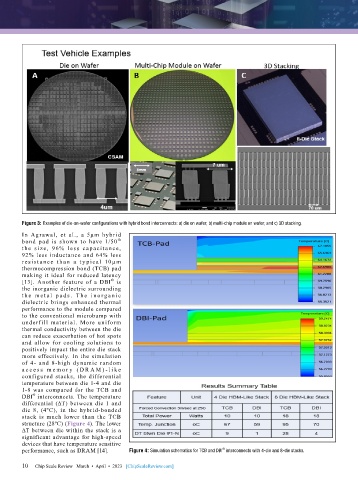
Figure 3: Examples of die-on-wafer configurations with hybrid bond interconnects: a) die on wafer; b) multi-chip module on wafer; and c) 3D stacking.
        In  Agrawal,  et  al.,  a  5μm  hybrid
                                        th
        bond pad is shown to have 1/50
        t he si z e, 96% le s s capa cit a nc e,
        92% less inductance and 64% less
        r e si s t a n c e t h a n a t y pic a l 10 µ m
        thermocompression bond (TCB) pad
        making it ideal for reduced latency
                                     ®
        [13]. Another feature of a DBI  is
        the inorganic dielectric surrounding
        t h e m e t a l p a d s . T h e i n o r g a n i c
        dielectric brings enhanced thermal
        performance to the module compared
        to the conventional microbump with
        underf ill material. More uniform
        thermal conductivity between the die
        can reduce exacerbation of hot spots
        and allow for cooling solutions to
        positively impact the entire die stack
        more effectively. In the simulation
        of 4- and 8-high dynamic random
        a c c e s s m e m o r y ( D R A M ) - l i k e
        configured stacks, the differential
        temperature between die 1-4 and die
        1-8 was compared for the TCB and
        DBI  interconnects. The temperature
            ®
        differential  (ΔT)  between  die  1  and
        die 8, (4ºC), in the hybrid-bonded
        stack is much lower than the TCB
        structure (28ºC) (Figure 4). The lower
        ΔT between die within the stack is a
        significant advantage for high-speed
        devices that have temperature sensitive
        performance, such as DRAM [14].    Figure 4: Simulation schematics for TCB and DBI  interconnects with 4-die and 8-die stacks.
                                                                          ®
        10
        10   Chip Scale Review   March  •  April  •  2023   [ChipScaleReview.com]

