Page 9 - Chip Scale Review_March April_2023-digital
P. 9
3D chiplet integration with hybrid bonding


        By Laura Mirkarimi  [Adeia, Inc.]

        M            arket demand for high-  stacks of memory on logic into products   Common Heterogeneous Integration and


                     performance computing
                                                                              (CHIPS) program was born. The goal of
                     (HPC) in server, gaming,   with assistance from foundries like   Intellectual Property (IP) Reuse Strategies
                                           TSMC and outsourced semiconductor
        artificial intelligence, and machine   assembly and test providers (OSATs) like   this program is to create a paradigm shift,
        learning applications is growing. In   ASE. The chiplet approach in 2.5D was   “to enhance overall system flexibility,
        2021, HPC was a $35B business and   shown to cost one-half of the comparable   reduce design time for next-generation
        is predicted to be $65B in 2030 with a   monolithic structure [2]. However, the   products, with significant IP reuse [5].”
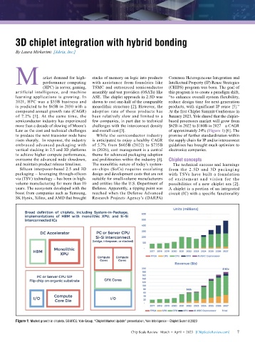
        compound annual growth rate (CAGR)   adoption rate of these products has   At the first Chiplet Summit Conference in
        of 7.2% [1]. At the same time, the   been relatively slow and limited to a   January 2023, Yole shared that the chiplet-
        semiconductor industry has experienced   few companies, in part due to technical   based processors market will grow from
        more than a decade of slowing of Moore’s   challenges with the interconnect density   $62B in 2022 to $180B in 2027—a CAGR
        Law as the cost and technical challenges   and overall cost [3].      of approximately 24% (Figure 1) [6]. The
        to produce the next transistor node have   While the semiconductor industry   promise of further standardization within
        risen sharply.  In response, the industry   is anticipated to enjoy a healthy CAGR   the supply chain for IP and/or interconnect
        embraced advanced packaging with   of 5.7% from $605B (2022) to $735B   guidelines has brought much optimism to
        vertical stacking in 2.5 and 3D platforms   in (2026), cost management is a central   electronics companies.
        to achieve higher compute performance,   theme for advanced packaging adoption
        overcome the advanced node slowdown,   and proliferation within the industry [4].   Chiplet concepts
        and maintain product release timelines.  The monolithic nature of today’s system-  The technical success and learnings
          Silicon interposer-based 2.5 and 3D   on-chips (SoCs) requires escalating   from the 2.5D and 3D packaging
        packaging – leveraging through-silicon   design and development costs that are not   with TSVs have built a foundation
        via (TSV) technology – has been in high-  suitable for small-volume manufacturers   of excitement and vision for the
        volume manufacturing for more than 10   and entities like the U.S. Department of   possibilities of a new chiplet era [2].
        years. The ecosystem developed with the   Defense. Apparently, a tipping point was   A chiplet is a portion of an integrated
        boost from companies such as Samsung,   reached when the Defense Advanced   circuit (IC) with a specific functionality
        SK Hynix, Xilinx, and AMD that brought   Research Projects Agency’s (DARPA)


        Figure 1: Market growth in chiplets. SOURCE: Yole Group, “Chiplet Market Update” presentation, Yole Intelligence - Chiplet Summit 2023

                                                             Chip Scale Review   March  •  April  •  2023   [ChipScaleReview.com]  7 7

