Page 16 - Chip Scale Review_March April_2023-digital
P. 16
There are several D2W bonding methods available for   The bonder should be capable of achieving sub-micron
        heterogeneous integration, each with its own advantages   alignment accuracy, and should also be able to handle
        and disadvantages, as shown in Table 1. Selecting the best   a high volume of dies for efficient production. The next
        approach for a given application depends on factors such as die   step involves transferring the dies from the carrier wafer
        size, thickness, total stack height, and interface considerations   to the product wafer. This is typically achieved through
        like contact design and density.                     W2W bonding using high-precision alignment and bonding
                                                             equipment. The bonding process should be performed under
                                                             controlled conditions to ensure uniformity and reliability.
                                                             After the dies have been transferred to the product wafer,
                                                             the die carrier is debonded and removed. This involves
                                                             separating the adhesive layer from the carrier wafer and
                                                             cleaning any residual adhesive from the product wafer. The
                                                             cleaning process should be carefully controlled to avoid
                                                             damage to the dies or product wafer.
                                                             Direct placement D2W hybrid bonding
                                                               D i r e c t d i e p l a c e m e n t  D 2 W h y b r i d b o n d i n g
        Table 1: Comparison between W2W and D2W hybrid bonding according to main
        decision criteria.                                   involves picking and placing a die onto a target wafer,
                                                             followed by annealing to covalently bond the dies and
        Collective D2W bonding process                       electrically  connect  them  [4].  The  first  step  in  this
          Collective D2W bonding involves the bonding of multiple   process is selecting a suitable die carrier, as shown in
        dies onto a wafer substrate in a highly accurate and reliable   Figure 3. Depending on the requirements of the application,
        manner. The collective D2W bonding process typically   the carrier can be a film frame or a specially-designed and
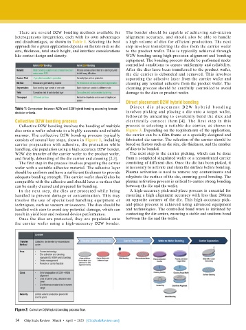
        consists of several key steps, shown in Figure 2, including   fabricated die carrier. The selection of the carrier should be
        carrier preparation with adhesive, die protection while   based on factors such as die size, die thickness, and the number
        handling, die population using a high accuracy D2W bonder,   of dies to be bonded.
        W2W die transfer of the carrier wafer to the product wafer,   The next step is the carrier picking, which can be done
        and finally, debonding of the die carrier and cleaning [2,3].  from a completed singulated wafer or a reconstituted carrier
          The first step in the process involves preparing the carrier   consisting of different dies. Once the die has been picked, it
        wafer with a suitable adhesive material. The adhesive layer   is necessary to activate and clean the surface before bonding.
        should be uniform and have a sufficient thickness to provide   Plasma activation is used to remove any contaminants and
        adequate bonding strength. The carrier wafer should also be   rehydrate the surface of the die, ensuring good bonding. The
        compatible with the adhesive and should have a surface that   plasma activation process is critical to ensure strong bonding
        can be easily cleaned and prepared for bonding.      between the die and the wafer.
          In the next step, the dies are protected while being   A high-accuracy pick-and-place process is essential for
        handled to prevent damage or contamination. This may   ensuring a high alignment accuracy with less than 200nm
        involve the use of specialized handling equipment or   on opposite corners of the die. This high-accuracy pick-
        techniques, such as vacuum or tweezers. The dies should be   and-place process is achieved using advanced equipment
        handled with care to avoid any potential damage, which can   and technologies. The controlled bond wave is initiated by
        result in yield loss and reduced device performance.  contacting the die center, ensuring a stable and uniform bond
          Once the dies are protected, they are populated onto   between the die and the wafer.
        the carrier wafer using a high-accuracy D2W bonder.


        Figure 2: Collective D2W hybrid bonding process flow.

        14
        14   Chip Scale Review   March  •  April  •  2023   [ChipScaleReview.com]

