Page 65 - Chip Scale Review_November December_2021-digital
P. 65
As systems grow, so must FOWLP flow


        By Keith Felton, John Ferguson  [Siemens EDA, a part of Siemens Digital Industries Software]
        A         s package-level integration


                  and complexity grow, so
                  do the required desig n
        iterations, costs, and manpower. Methods
        that worked in the past are not scaling
        and are therefore resulting in adoption
        challenges. Monolithic advanced-node
        single-chip packaging is no longer the
        solution for emerging market demands
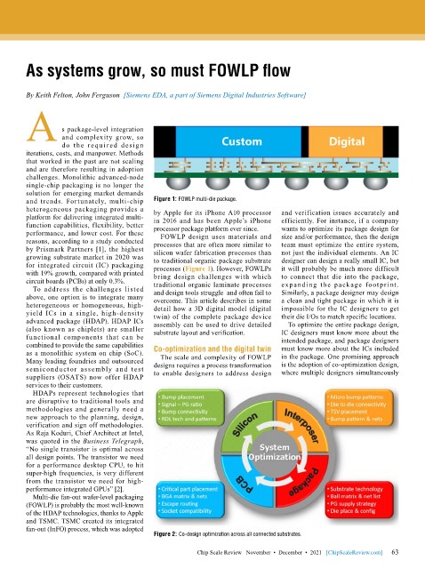
        and trends. Fortunately, multi-chip   Figure 1: FOWLP multi-die package.
        heterogeneous packaging provides a   by Apple for its iPhone A10 processor   and verification issues accurately and
        platform for delivering integrated multi-  in 2016 and has been Apple’s iPhone   efficiently. For instance, if a company
        function capabilities, flexibility, better   processor package platform ever since.  wants to optimize its package design for
        performance, and lower cost. For these   FOWLP design uses materials and   size and/or performance, then the design
        reasons, according to a study conducted   processes that are often more similar to   team must optimize the entire system,
        by Prismark Partners [1], the highest   silicon wafer fabrication processes than   not just the individual elements. An IC
        growing substrate market in 2020 was   to traditional organic package substrate   designer can design a really small IC, but
        for integrated circuit (IC) packaging   processes (Figure 1). However, FOWLPs   it will probably be much more difficult
        with 19% growth, compared with printed   bring design challenges with which   to connect that die into the package,
        circuit boards (PCBs) at only 0.3%.  traditional organic laminate processes   expanding the package footprint.
          To address  the  challenges listed   and design tools struggle  and often fail to   Similarly, a package designer may design
        above, one option is to integrate many   overcome. This article describes in some   a clean and tight package in which it is
        heterogeneous or homogeneous, high-  detail how a 3D digital model (digital   impossible for the IC designers to get
        yield ICs in a single, high-density   twin) of the complete package device   their die I/Os to match specific locations.
        advanced package (HDAP). HDAP ICs   assembly can be used to drive detailed   To optimize the entire package design,
        (also known as chiplets) are smaller   substrate layout and verification.   IC designers must know more about the
        functional components that can be                                     intended package, and package designers
        combined to provide the same capabilities                             must know more about the ICs included
        as a monolithic system on chip (SoC).   Co-optimization and the digital twin  in the package. One promising approach
        Many leading foundries and outsourced   The scale and complexity of FOWLP   is the adoption of co-optimization design,
        semiconductor assembly and test    designs requires a process transformation   where multiple designers simultaneously
        suppliers (OSATS) now offer HDAP   to enable designers to address design
        services to their customers.
          HDAPs represent technologies that
        are disruptive to traditional tools and
        methodologies and generally need a
        new approach to the planning, design,
        verification and sign off methodologies.
        As Raja Koduri, Chief Architect at Intel,
        was quoted in the Business Telegraph,
        “No single transistor is optimal across
        all design points. The transistor we need
        for a performance desktop CPU, to hit
        super-high frequencies, is very different
        from the transistor we need for high-
        performance integrated GPUs” [2].
          Multi-die fan-out wafer-level packaging
        (FOWLP) is probably the most well-known
        of the HDAP technologies, thanks to Apple
        and TSMC. TSMC created its integrated
        fan-out (InFO) process, which was adopted
                                           Figure 2: Co-design optimization across all connected substrates.

                                                                                                             63
                                                       Chip Scale Review   November  •  December  •  2021   [ChipScaleReview.com]  63

