Page 68 - Chip Scale Review_November December_2021-digital
P. 68
exceed 250,000. Such levels of validation   perform the critical checks noted above   with packaging design tools. Typically,
        and verification are commonplace in chip   exists today, it has to be integrated into   the required checks fall into two
        design but are a new phenomenon for   the package design flow and process.   categories: physical (geometric) and
        package designers.                 Ideally, it also must be capable of   electrical connectivity.
          Although the technology needed to   providing results that can be displayed   Physical verification of FOWLP
                                                                              designs must address the unique physical
                                                                              characteristics of these packages, including
                                                                              the presence of multiple components,
                                                                              non-Manhattan shapes, and disparate file
                                                                              standards. Fortunately, FOWLP designers
                                                                              do not need to check every geometry in
                                                                              every die. Each individual die in a FOWLP
                                                                              package is already taped out for its target
                                                                              foundry with respect to DRC and LVS
                                                                              comparisons. FOWLP verification does
                                                                              require designers to check the interactions
                                                                              between the dies, which may require
                                                                              extracting several layers within each die
                                                                              to see what their impacts are on each other
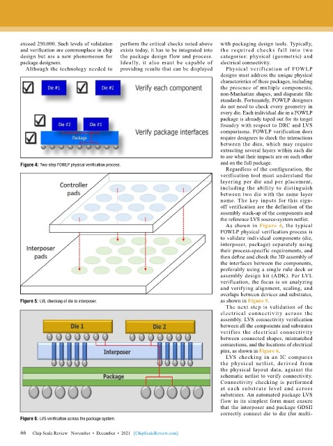
        Figure 4: Two-step FOWLP physical verification process.               and on the full package.
                                                                                Regardless of the configuration, the
                                                                              verification tool must understand the
                                                                              layering per die and per placement,
                                                                              including the ability to distinguish
                                                                              between two die with the same layer
                                                                              name. The key inputs for this sign-
                                                                              off verification are the definition of the
                                                                              assembly stack-up of the components and
                                                                              the reference LVS source-system netlist.
                                                                                As shown in Figure 4, the typical
                                                                              FOWLP physical verification process is
                                                                              to validate individual components (die,
                                                                              interposer, package) separately using
                                                                              their process-specific requirements, and
                                                                              then define and check the 3D assembly of
                                                                              the interfaces between the components,
                                                                              preferably using a single rule deck or
                                                                              assembly design kit (ADK). For LVL
                                                                              verification, the focus is on analyzing
                                                                              and verifying alignment, scaling, and
                                                                              overlaps between devices and substrates,
        Figure 5: LVL checking of die to interposer.                          as shown in Figure 5.
                                                                                The next step is validation of the
                                                                              electrical connectivity across the
                                                                              assembly. LVS connectivity verification
                                                                              between all the components and substrates
                                                                              verifies the electrical connectivity
                                                                              between connected shapes, mismatched
                                                                              connections, and the locations of electrical
                                                                              pins, as shown in Figure 6.
                                                                                LVS checking in an IC compares
                                                                              the physical netlist, derived from
                                                                              the physical layout data, against the
                                                                              schematic netlist to verify connectivity.
                                                                              Connectivity checking is performed
                                                                              at each substrate level and across
                                                                              substrates. An automated package LVS
                                                                              flow in its simplest form must ensure
                                                                              that the interposer and package GDSII
                                                                              correctly connect die to die (for multi-
        Figure 6: LVS verification across the package system.

        66
        66   Chip Scale Review   November  •  December  •  2021   [ChipScaleReview.com]

