Page 39 - Chip Scale Review_November December_2021-digital
P. 39
Introducing hybrid graphene/metal structures in the


        BEOL technology roadmap


        By Swati Achra, Inge Asselberghs, Zsolt Tokei  [imec]
        A         dvanced scaling in the


                  front-end-of-line (FEOL)
                  needs to go hand in hand
        with innovations in the back-end-of-line
        (BEOL)—the network of interconnects
        t hat  con ne ct s  sea m le ssly  t o  t he
        underlying device structures. This BEOL
        is organized in different metal layers
        (local, intermediate, semi-global and
        global) that are vertically-interconnected
        by means of via structures – filled
        with metals. Today, Cu-based dual-
        damascene is the workhorse process flow
        for making the interconnects. But with
        each new technology generation, routing
        congestion and a dramatic signal delay
        (resulting from an increased resistance-
        capacitance (RC) product) become
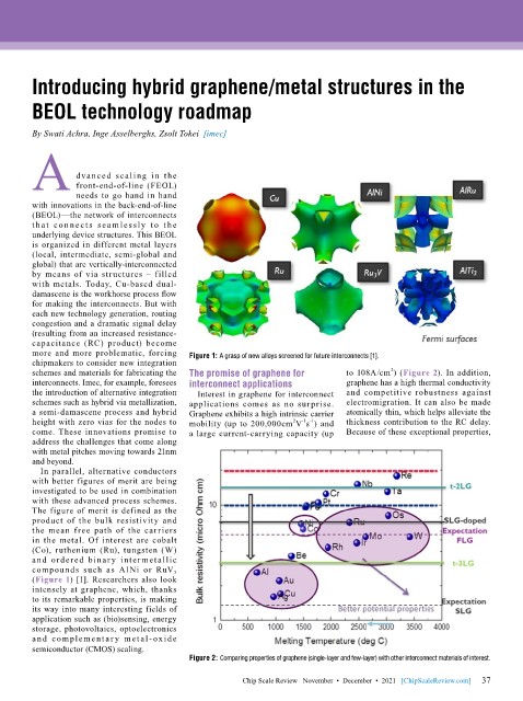
        more and more problematic, forcing   Figure 1: A grasp of new alloys screened for future interconnects [1].
        chipmakers to consider new integration
                                                                                        2
        schemes and materials for fabricating the   The promise of graphene for   to 108A/cm ) (Figure 2). In addition,
        interconnects. Imec, for example, foresees   interconnect applications  graphene has a high thermal conductivity
        the introduction of alternative integration   Interest in graphene for interconnect   and competitive robustness against
        schemes such as hybrid via metallization,   applications comes as no surprise.   electromigration. It can also be made
        a semi-damascene process and hybrid   Graphene exhibits a high intrinsic carrier   atomically thin, which helps alleviate the
        height with zero vias for the nodes to   mobility (up to 200,000cm V s ) and   thickness contribution to the RC delay.
                                                                   2
                                                                     -1 -1
        come. These innovations promise to   a large current-carrying capacity (up   Because of these exceptional properties,
        address the challenges that come along
        with metal pitches moving towards 21nm
        and beyond.
          In parallel, alternative conductors
        with better figures of merit are being
        investigated to be used in combination
        with these advanced process schemes.
        The figure of merit is defined as the
        product of the bulk resistivity and
        the  mean  free path  of  the carriers
        in the metal. Of interest are cobalt
        (Co), ruthenium (Ru), tungsten (W)
        and ordered binar y inter metallic
        compounds such as AlNi or RuV 3
        (Figure 1) [1]. Researchers also look
        intensely at graphene, which, thanks
        to its remarkable properties, is making
        its way into many interesting fields of
        application such as (bio)sensing, energy
        storage, photovoltaics, optoelectronics
        a nd complement a r y met al- ox ide
        semiconductor (CMOS) scaling.
                                           Figure 2: Comparing properties of graphene (single-layer and few-layer) with other interconnect materials of interest.

                                                                                                             37
                                                       Chip Scale Review   November  •  December  •  2021   [ChipScaleReview.com]  37

