Page 35 - Chip Scale Review_November December_2021-digital
P. 35
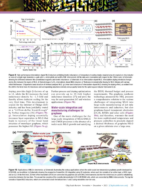
Figure 9: High-performance intercalation-doped MLG inductors exhibiting kinetic inductance: a) Comparison of scaling trends: required area of a typical on-chip inductor
        vs. area of a single logic transistor (= gate pitch × metal pitch) and width of M1 interconnect. All the data were normalized with respect to the 130nm node. b) Schematic
        showing the difference between the conventional magnetic and kinetic inductance. c) Schematic of an intercalation-doped MLG. Intercalation doping introduces foreign
        atoms (Br 2 ) between the layers of MLG. d) Optical image of a Br 2  intercalation-doped MLG inductor. e) Thickness increment after doping for MLG ribbons with various
        initial thicknesses. f) Hyperbolic band structure of intrinsic/undoped MLG. g) Linear band structure of intercalation-doped MLG showing the doping effect, as evident from
        the shift in the fermi level. h) Inductance and corresponding inductance density versus quality factor for the spiral square inductor fabricated in (d).
        doping provides high Q-factors of up   Further process and doping optimization   the BEOL thermal budget and process
        to 12, while the KI increases the total   can provide up to 10-fold higher   requirements. The graphene synthesis
        inductance-density by ~1.5-fold and   inductance densities [17] and pave the   technology pioneered by NRL presents
        thereby allows inductor scaling for the   way for next-generation IoT and wireless     a comprehensive solution to the various
        very first time. This development is   applications (Figure 9h).      challenges of integrating MLG into
        crucial for the Internet of Things (IoT)                              large-scale manufacturing of not only
        industry and has been justifiably touted   Wafer-scale integration and   interconnects and inductors, but also
        as a “trillion-dollar breakthrough”   manufacturing challenges for    graphene-based transparent electrodes
        by Forbes magazine [16] (Figure 9b-  graphene                         [14,18], RFIDs and solar cells (Figure
        g). Intercalation doping essentially   One of the main challenges for the   10a), and therefore, warrants the need
        increases layer separation in MLG that   large-scale integration of MLG/DMLG   for more sophisticated temperature and
        leads to recovery of the linear band   into CMOS processes is the absence of a   pressure controllers to precisely deposit
        structure of monolayer graphene, which   wafer-scale MLG growth tool satisfying   a desired thickness of graphene/MLG
        possesses the highest KI (Figure 9e-g).                               on a given substrate over a large area.


        Figure 10: Applications of MLG in electronics: a) Schematic illustrating the various applications where the wafer-scale low-temperature graphene growth developed by
        UCSB NRL can be utilized. b) Schematic showing the prospects of monolithic 3D integration using 2D materials, where each tier consists of an active layer, a BEOL layer
        and an ILD. At the first level, 2D field-effect transistors (FETs) are connected via graphene (Gr) and DMLG interconnects and inter-tier metal vias are used for establishing
        connection between the two tiers. The second tier consists of the recently demonstrated 0.5T-0.5R RRAM cells, which are connected by DMLG interconnects. The top tier
        consists of doped MLG inductors, which are connected to both the bottom tiers 1 and 2 using monolithic inter-tier vias.

                                                                                                             33
                                                       Chip Scale Review   November  •  December  •  2021   [ChipScaleReview.com]  33

