Page 33 - Chip Scale Review_November December_2021-digital
P. 33
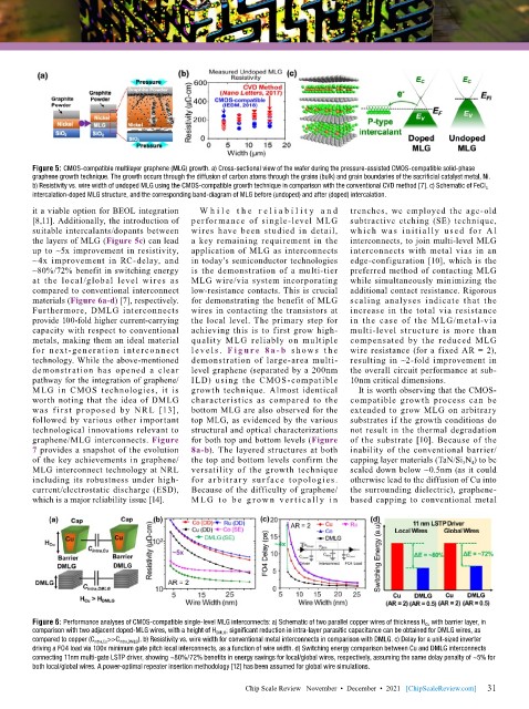
Figure 5: CMOS-compatible multilayer graphene (MLG) growth. a) Cross-sectional view of the wafer during the pressure-assisted CMOS-compatible solid-phase
        graphene growth technique. The growth occurs through the diffusion of carbon atoms through the grains (bulk) and grain boundaries of the sacrificial catalyst metal, Ni.
        b) Resistivity vs. wire width of undoped MLG using the CMOS-compatible growth technique in comparison with the conventional CVD method [7]. c) Schematic of FeCl 3
        intercalation-doped MLG structure, and the corresponding band-diagram of MLG before (undoped) and after (doped) intercalation.
        it a viable option for BEOL integration   W h i l e  t h e  r e l i a b i l i t y  a n d   trenches, we employed the age-old
        [8,11]. Additionally, the introduction of   performance of  single-level MLG   subtractive etching (SE) technique,
        suitable intercalants/dopants between   wires have been studied in detail,   wh ich wa s i n it ial ly u sed for A l
        the layers of MLG (Figure 5c) can lead   a key remaining requirement in the   interconnects, to join multi-level MLG
        up to ~5x improvement in resistivity,   application of MLG as interconnects   interconnects with metal vias in an
        ~4x improvement in RC-delay, and   in today’s semiconductor technologies   edge-configuration [10], which is the
        ~80%/72% benefit in switching energy   is the demonstration of a multi-tier   preferred method of contacting MLG
        at the local/global level wires as   MLG wire/via system incorporating   while simultaneously minimizing the
        compared to conventional interconnect   low-resistance contacts. This is crucial   additional contact resistance. Rigorous
        materials (Figure 6a-d) [7], respectively.   for demonstrating the benefit of MLG   scaling analyses indicate that the
        Furthermore, DMLG interconnects    wires in contacting the transistors at   increase in the total via resistance
        provide 100-fold higher current-carrying   the local level. The primary step for   in  the case of the  MLG/metal-via
        capacity with respect to conventional   achieving this is to first grow high-  multi-level structure is more than
        metals, making them an ideal material   quality MLG reliably on multiple   compensated by the reduced MLG
        for next-generation intercon nect   l e ve l s .   Fi g u r e  8 a -b  s how s t h e   wire resistance (for a fixed AR = 2),
        technology. While the above-mentioned   demonstration  of  large-area  multi-  resulting in ~2-fold improvement in
        demonstration has opened a clear   level graphene (separated by a 200nm   the overall circuit performance at sub-
        pathway for the integration of graphene/  ILD) using the CMOS-compatible   10nm critical dimensions.
        MLG in CMOS technologies, it is    growth technique. Almost identical   It is worth observing that the CMOS-
        worth noting that the idea of DMLG   characteristics as compared to the   compatible growth process can be
        was f irst proposed by NR L [13],   bottom MLG are also observed for the   extended to grow MLG on arbitrary
        followed by various other important   top MLG, as evidenced by the various   substrates if the growth conditions do
        technological innovations relevant to   structural and optical characterizations   not result in the thermal degradation
        graphene/MLG interconnects. Figure   for both top and bottom levels (Figure   of the substrate [10]. Because of the
        7 provides a snapshot of the evolution   8a-b). The layered structures at both   inability of the conventional barrier/
        of the key achievements in graphene/  the top and bottom levels confirm the   capping layer materials (TaN/Si 3 N 4 ) to be
        MLG interconnect technology at NRL   versatility of the growth technique   scaled down below ~0.5nm (as it could
        including its robustness under high-  for arbit rar y su rface topologies.   otherwise lead to the diffusion of Cu into
        current/electrostatic discharge (ESD),   Because of the difficulty of graphene/  the surrounding dielectric), graphene-
        which is a major reliability issue [14].  M L G t o b e g r ow n ve r t ic a l ly i n   based capping to conventional metal


        Figure 6: Performance analyses of CMOS-compatible single-level MLG interconnects: a) Schematic of two parallel copper wires of thickness H Cu  with barrier layer, in
        comparison with two adjacent doped-MLG wires, with a height of H DMLG ; significant reduction in intra-layer parasitic capacitance can be obtained for DMLG wires, as
        compared to copper (C intra,Cu >>C intra,DMLG ). b) Resistivity vs. wire width for conventional metal interconnects in comparison with DMLG. c) Delay for a unit-sized inverter
        driving a FO4 load via 100x minimum gate pitch local interconnects, as a function of wire width. d) Switching energy comparison between Cu and DMLG interconnects
        connecting 11nm multi-gate LSTP driver, showing ~80%/72% benefits in energy savings for local/global wires, respectively, assuming the same delay penalty of ~5% for
        both local/global wires. A power-optimal repeater insertion methodology [12] has been assumed for global wire simulations.

                                                                                                             31
                                                       Chip Scale Review   November  •  December  •  2021   [ChipScaleReview.com]  31

