Page 28 - Chip Scale Review_November December_2021-digital
P. 28
Sustaining Moore’s Law with graphene


        By Kunjesh Agashiwala, Junkai Jiang, Ankit Kumar, Chao-Hui Yeh, Kaustav Banerjee  [University of California, Santa Barbara]
        S        ince the invention of metal-  Scaling limitations of conventional   requirements set forth by the International


                 oxide-semiconductor (MOS)
                 integrated circuits in the   interconnect materials          Roadmap for Devices and Systems (IRDS)
                                                                              beyond 15nm wiring dimensions, as shown
                                             Even though cobalt (Co) has recently
        early 1960s, the speed, capacity, and   been introduced as a possible substitute   in Figure 2d, necessitating an urgent
        complexity of the chips have increased   for the narrowest Cu lines to keep   need to identify alternative metallization
        dramatically, roughly following Moore’s   Moore’s Law alive, these technologies   strategies to keep Moore’s Law alive.
        Law, owing to various technological   will eventually run out of steam when
        and process breakthroughs that doubled   wiring dimensions approach sub-20nm.   What is so exciting about graphene
        the transistor count per chip area every   At these critical dimensions, conventional   interconnects?
        two to three years. Along with the   technologies such as Cu, Co, and noble   Since its discovery in 2004 [4], graphene
        advancement in transistor technology,   metals such as ruthenium (Ru) suffer   has been proposed as a potential material
        the wires (or interconnects) that connect   from significant size effects, mainly due   for future electronics because of its
        these billions of transistors have   to a nonlinear increase in resistivity, and   unique electrical, optical, and mechanical
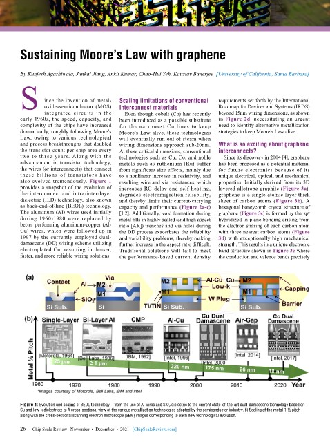
        also evolved tremendously. Figure 1   resulting wire and via resistances, which   properties. Initially derived from its 3D
        provides a snapshot of the evolution of   increases RC-delay and self-heating,   layered allotrope-graphite (Figure 3a),
        the interconnect and intra/inter-layer   degrades electromigration reliability,   graphene is a single atomic-layer-thick
        dielectric (ILD) technology, also known   and thereby limits their current-carrying   sheet of carbon atoms (Figure 3b). A
        as back-end-of-line (BEOL) technology.   capacity and performance (Figure 2a-c)   hexagonal honeycomb crystal structure of
        The aluminum (Al) wires used initially   [1,2]. Additionally, void formation during   graphene (Figure 3c) is formed by the sp
                                                                                                              2
        during 1960-1980 were replaced by   metal fills in highly scaled (and high aspect   hybridized in-plane bonding arising from
        better performing aluminum-copper (Al-  ratio [AR]) trenches and via holes during   the electron sharing of each carbon atom
        Cu) wires, which were followed up in   the DD process exacerbates the reliability   with three nearest carbon atoms (Figure
        1997 by the currently employed dual-  and variability problems, thereby making   3d) with exceptionally high mechanical
        damascene (DD) wiring scheme utilizing   further increase in the aspect ratio difficult.   strength. This results in a unique electronic
        electroplated Cu, resulting in denser,   Traditional solutions will fail to meet   band-structure shown in Figure 3e where
        faster, and more reliable wiring solutions.   the performance-based current density   the conduction and valence bands precisely


        Figure 1: Evolution and scaling of BEOL technology—from the use of Al wires and SiO 2  dielectric to the current state-of-the-art dual-damascene technology based on
        Cu and low-k dielectrics: a) A cross-sectional view of the various metallization technologies adopted by the semiconductor industry. b) Scaling of the metal-1 ½ pitch
        along with the cross-sectional scanning electron microscope (SEM) images corresponding to each new technological evolution.

        26   Chip Scale Review   November  •  December  •  2021   [ChipScaleReview.com]
        26

