Page 23 - Chip Scale Review_November December_2021-digital
P. 23
environments, typically experienced
        for electronics in close proximity to the
        engine, transmission, or braking systems.
          Similar reliability data were also
        collected for the C40 nm test vehicle,
        again leveraging the 172-lead MaxQFP.
        These data are detailed in Table 2. This
        test vehicle also passed 2X AEC Grade 1
        requirements. As before, multiple assembly
        lots were used for each stress test.
          In addition to the raw results noted
        above, post-stress scanning acoustic
        microscopy (SAM) images were taken
        to look for any package delamination.
        Examples of SAM images of post-TC
        1,000- and 2,000-cycle data are shown in
        Figure 5. In all cases, no delamination
        violating AEC requirements was
        observed on the test vehicles. Also, post-
        stress decapsulation wire pull and ball
        shear tests were performed. All passed
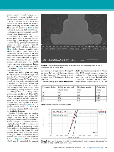
        AEC Q006 requirements. Cross-section
        scanning electron microscope (SEM)
        images were also taken to assure that the
        ball bonds have no Cu-Al intermetallic   Figure 6: Cross section/SEM image of Cu ball bonds of post-HTSL 2016 hrs showing no sign of Cu-Al IMC
        degradation (Figure 6) [1,2] and no Cu   degradation and no Cu void formation.
        void formation [3,4].              automotive SJR requirement. Design D   study. Because the solder joints of J-leads
          Board-level solder joint reliability.   performs the best—not showing a failure   after PCB mounting reside under the
        MaxQFP uses the same PCB design rules   on the J-leads until 9,791 cycles. It is the   package body, they are not inspectable
        as a standard 0.5mm pitch QFP—namely   recommended PCB footprint design for   with legacy AOI systems that only offer
        0.1/0.1mm line/space [5]. Therefore, even   MaxQFP.                   a top view. Therefore, for solder joint
        though the interstitial pitch of the leads   Automated optical inspection system   inspection of MaxQFP (or a PLCC, for
        is smaller, no finer-pitch (higher cost)
        PCB manufacturing is required to design
        with MaxQFP. Board-level SJR data were
        collected using a daisy chain die in a 172-
        lead MaxQFP under the temperature
        cycling stress condition of -40 to 125ºC.
        Cycling was continued until at least 50%
        of the parts failed, thereby enabling a
        statistical view of reliability performance.
        For this study, four separate PCB board
        footprints were designed (Table 3). The   Table 3: Four PCB footprints explored for MaxQFP.
        general automotive board-level SJR
        requirement is to pass 2,000 cycles before
        the first fail is detected.
          Design A is the baseline design,
        which is identical to the existing PCB
 Move faster with agile   footprint for both QFP gull-wing leads
        and plastic-leaded chip carrier (PLCC)
 PCB manufacturing  J-leads. Design B shares the same lead
        length of design A with an increased pad
        width. Design C is an aggressive, shorter,
        footprint length, but has been eliminated
        because it cannot be detected by AOI
        systems. Design D is a modified version
        of design C, which is inspectable by AOI
 PCB manufacturers that use data to drive decisions move   systems. The board-level SJR results are
 faster than competitors and reduce production costs.   plotted in Figure 7. All three footprints
 Learn how to adopt advanced manufacturing strategies to   (A, B, and D) exceeded the general   Figure 7: Board-level TC stresses (-40 to +125ºC) results for designs A, B, and D using daisy chain samples. The
 transform complex data into a unified digital thread.  Scan for    first failure on design D is 9,791 cycles on the J-lead.
 the eBook
                                                                                                             21
                                                       Chip Scale Review   November  •  December  •  2021   [ChipScaleReview.com]  21

