Page 19 - Chip Scale Review_November December_2021-digital
P. 19
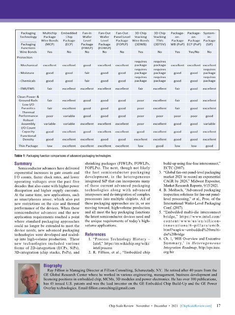
Table 1: Packaging function comparisons of advanced packaging technologies.
        Summary                            shrinking packages (FIWLPs, FOWLPs,    build-up using fine-line interconnect,”
          Semiconductor advances have delivered   FOPLPs). The next, though not likely   ECTC (2007).
        exponential increases in gate counts and   the last semiconductor packaging   3.  “Global fan-out panel-level packaging
        I/O counts, faster clock rates, and lower   development, is the heterogeneous   market 2021 to record an exponential
        operating voltages over the past five   integrated SiP that can incorporate many   CAGR by 2026,” Midwest Expositor,
        decades that also came with higher power   of these current advanced packaging   Market Research Reports, 9/15/2021.
        dissipation and higher supply currents.   technologies along with advanced   4.  B. Meihach, “Advanced packaging
        At the same time, new applications, such   interposers and de-integration of complex   inspection solutions for fan-out panel-
        as smartphones arose, which also put   processors into multiple chiplets. All of   level processing,” et al., Proc. of the
        new restrictions on the size and thermal   these packaging approaches are in, or are   International Wafer-Level Packaging
        performance of the devices. When these   moving toward, high-volume production   Conf. (2017).
        semiconductor advances and the new   and all meet the key packaging functions   5.  “Embedded multi-die interconnect
        application requirements reached a point   the latest semiconductor devices need and   bridge,”  https://www.intel.com/
        where standard packaging approaches   the unique requirements of today’s high-  c o nt e nt /w w w/ u s /e n /si l ic o n -
        could no longer be extended to meet the   volume applications.            i n n ov a t ion s /6 - pi l l a r s /e m ib.
        device needs, new advanced packaging                                      html?wapkw=embedded%20multi-
        technologies were developed and scaled-  References                       die%20bridge
        up into high-volume production.  These   1.  “Process Technology History –   6.  Ch. 1, ‘HIR Overview and Executive
        new  technologies  included  various   Intel,” https://en.wikichip.org/wiki/  Summar y,’  in  Heterogeneous
        forms of 2D-integration (ECPs, SiPs),   intel/process                     Integration Roadmap, http://eps.ieee.
        3D-integration (chip stacks, PoPs), and   2.  R. Fillion, et al., “Embedded chip   org/hir


                       Biography
                         Ray Fillion is Managing Director at Fillion Consulting, Schenectady, NY.  He retired after 40 years from the
                       GE Global Research Center where he worked in various engineering, management, business development and
                       licensing positions in embedded chip, MCMs, 3D modules and power electronics. He has over 100 publications,
                       has 45 issued U.S. patents and was the lead inventor on the GE Embedded Chip Build-Up and the GE Power
                       Overlay technologies. Email fillion.consulting@gmail.com


                                                                                                             17
                                                       Chip Scale Review   November  •  December  •  2021   [ChipScaleReview.com]  17

