Page 17 - Chip Scale Review_November December_2021-digital
P. 17
System-in-package (SiP)
          O n e o f t h e l a t e s t p a c k a g i ng
        development areas is the system-in-
        package (SiP). SiP is a combination of
        multiple active electronic components
        of different functionality, assembled
        in a single unit that provides multiple
        functions associated with a system or
        sub-system (JEDEC). A SiP generally
        contains processor chip, memory chips,
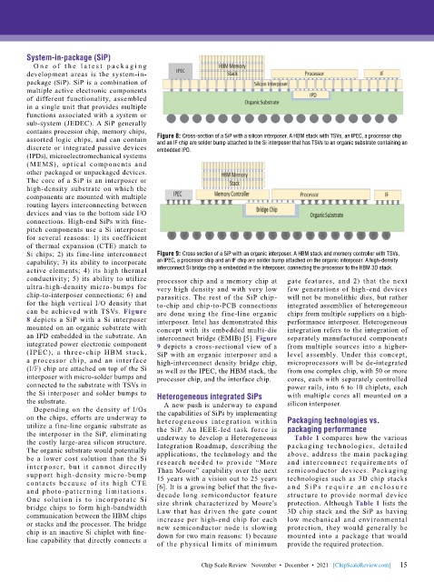
        assorted logic chips, and can contain   Figure 8: Cross-section of a SiP with a silicon interposer. A HBM stack with TSVs, an IPEC, a processor chip
                                           and an IF chip are solder bump attached to the Si interposer that has TSVs to an organic substrate containing an
        discrete or integrated passive devices   embedded IPD.
        (IPDs), microelectromechanical systems
        (MEMS), optical components and
        other packaged or unpackaged devices.
        The core of a SiP is an interposer or
        high-density substrate on which the
        components are mounted with multiple
        routing layers interconnecting between
        devices and vias to the bottom side I/O
        connections. High-end SiPs with fine-
        pitch components use a Si interposer
        for several reasons: 1) its coefficient
        of thermal expansion (CTE) match to
        Si chips; 2) its fine-line interconnect   Figure 9: Cross section of a SiP with an organic interposer. A HBM stack and memory controller with TSVs,
        capability; 3) its ability to incorporate   an IPEC, a processor chip and an IF chip are solder bump attached on the organic interposer. A high-density
        active elements; 4) its  high  thermal   interconnect Si bridge chip is embedded in the interposer, connecting the processor to the HBM 3D stack.
        conductivity; 5) its ability to utilize   processor chip and a memory chip at   gate features, and 2) that the next
        ultra-high-density micro-bumps for   very high density and with very low   few generations of high-end devices
        chip-to-interposer connections; 6) and   parasitics. The rest of the SiP chip-  will not be monolithic dies, but rather
        for the high vertical I/O density that   to-chip and chip-to-PCB connections   integrated assemblies of heterogeneous
        can be achieved with TSVs.  Figure   are done using the fine-line organic   chips from multiple suppliers on a high-
        8 depicts a SiP with a Si interposer   interposer. Intel has demonstrated this   performance interposer. Heterogeneous
        mounted on an organic substrate with   concept with its embedded multi-die   integration refers to the integration of
        an IPD embedded in the substrate. An   interconnect bridge (EMIB) [5]. Figure   separately manufactured components
        integrated power electronic component   9 depicts a cross-sectional view of a   from multiple sources into a higher-
        (IPEC), a three-chip HBM stack,    SiP with an organic interposer and a   level assembly. Under this concept,
        a processor chip, and an interface     high-interconnect density bridge chip,   microprocessors will be de-integrated
        (I/F) chip are attached on top of the Si   as well as the IPEC, the HBM stack, the   from one complex chip, with 50 or more
        interposer with micro-solder bumps and   processor chip, and the interface chip.  cores, each with separately controlled
        connected to the substrate with TSVs in                               power rails, into 6 to 10 chiplets, each
        the Si interposer and solder bumps to   Heterogeneous integrated SiPs  with multiple cores all mounted on a
        the substrate.                       A new push is underway to expand   silicon interposer.
          Depending on the density of I/Os   the capabilities of SiPs by implementing
        on the chips, efforts are underway to   heterogeneous integration within   Packaging technologies vs.
        utilize a fine-line organic substrate as   the SiP. An IEEE-led task force is   packaging performance
        the interposer in the SiP, eliminating   underway to develop a Heterogeneous   Table 1 compares how the various
        the costly large-area silicon structure.   Integration Roadmap, describing the   packaging technologies, detailed
        The organic substrate would potentially   applications, the technology and the   above, address the main packaging
        be a lower cost solution than the Si   research needed to provide “More   and interconnect requirements of
        inter poser, but it cannot directly   Than Moore” capability over the next   semiconductor devices. Packaging
        support high-density micro-bump    15 years with a vision out to 25 years   technologies such as 3D chip stacks
        contacts because of its high CTE   [6]. It is a growing belief that the five-  a n d S i P s r e q u i r e a n e n c l o s u r e
        and photo-patterning limitations.   decade long semiconductor feature   structure to provide normal device
        One solution is to incor porate Si   size shrink characterized by Moore’s   protection. Although Table 1 lists the
        bridge chips to form high-bandwidth   Law that has driven the gate count   3D chip stack and the SiP as having
        communication between the HBM chips   increase per high-end chip for each   low mechanical and environmental
        or stacks and the processor. The bridge   new semiconductor node is slowing   protection, they would generally be
        chip is an inactive Si chiplet with fine-  down for two main reasons: 1) because   mounted into a package that would
        line capability that directly connects a   of the physical limits of minimum   provide the required protection.


                                                                                                             15
                                                       Chip Scale Review   November  •  December  •  2021   [ChipScaleReview.com]  15

