
Page 12 - Chip Scale Review_November December_2021-digital
P. 12
Advanced microelectronics packaging technologies
and their performance
By Ray Fillion [Fillion Consulting]
N ew packaging technologies Semiconductor advancements bonds to solder bumps, from perimeter
are developed for one
Semiconductor wafer fabrication
of two reasons: either to capabilities as measured in minimum leads to ball grid array (BGA), from
2D assemblies to 3D assemblies, and
address advances in semiconductor gate width or minimum line width, from single-chip packaging to multi-
device technology, such as higher I/O have been the main driving force for chip modules (MCMs). The following
counts, faster clock rates, higher power semiconductor device advancements paragraphs will look at the latest
dissipation and lower operating voltages; for the past f ive decades. These advanced packaging technologies.
or to meet the requirements of new advancements were due to improved
application areas, such as smartphones phot ol it hog r a phy, mor e p r e ci s e Embedded chip packaging
or implantable medical devices. Any equipment, cleaner fab spaces, innovative Embedded chip packaging (ECP)
new packaging development must materials, and new device structures. was developed as a high-performance
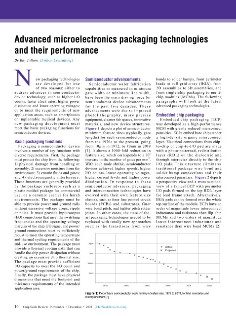
meet the basic packaging functions for Figure 1 depicts a plot of semiconductor MCM with greatly reduced interconnect
semiconductor devices. minimum feature sizes (typically gate parasitics. ECPs embed bare chips under
lengths) for each semiconductor node a high-density organic interconnect
Basic packaging functions from the 1970s to the present, going layer. Electrical connections from chip-
Packaging a semiconductor device from 10µm in 1972, to 10nm in 2019 to-chip or chip-to-I/O pad are made
involves a number of key functions with [1]. It shows a 1000-fold reduction in with a photo-patterned, redistribution
6
diverse requirements. First, the package feature size, which corresponds to a 10 layer (RDL) on the dielectric and
2
must protect the chip from the following: increase in the number of gates per mm . through microvias directly to the chip
1) physical damage from handling or With each node shrink, semiconductor I/O pads. This structure eliminates
assembly; 2) excessive moisture from the devices achieved higher speeds, higher traditional package wire bond and
environment; 3) caustic fluids and gases; I/O counts, lower operating voltages, solder bump connections and their
and 4) electromagnetic interference. higher current levels and higher power interconnect parasitics. Figure 2 depicts
These functions are generally provided dissipation. In response to these a perspective view and a cross-sectional
by the package enclosure such as a semiconductor advances, packaging view of a typical ECP with perimeter
plastic molded package for commercial and interconnection technologies have I/O pads formed on the top RDL layer
use, or a ceramic carrier for harsh evolved with their own feature size for lead frame attach. Alternatively,
environments. The package must be shrinks, such as finer line printed circuit BGA pads can be formed over the whole
able to provide power and ground rails boards (PCBs) and substrates, finer top surface of the module. ECPs have an
without excessive voltage drops, ripple wire bond pitch, and tighter pitch solder order of magnitude lower interconnect
or noise. It must provide input/output joints. In other cases, the state-of-the- inductance and resistance than flip-chip
(I/O) connections that meet the switching art packaging technologies needed to be MCMs and two orders of magnitude
frequencies and the operating voltage replaced with totally new approaches lower interconnect inductance and
margins of the chip. I/O signal and power/ such as the transitions from wire resistance than wire bond MCMs [2].
ground connections must be sufficiently
robust to meet the operating temperature
and thermal cycling requirements of the
end-use environment. The package must
provide a thermal cooling path that can
handle the chip power dissipation without
creating an excessive chip thermal rise.
The package must provide sufficient
I/O capacity to meet the I/O count and
power/ground requirements of the chip.
Finally, the package must have physical
dimensions that meet the footprint and
thickness requirements of the intended
application area.
Figure 1: Plot of basic semiconductor node minimum feature size, 1972 to 2019, for Intel memories and
microprocessors [2].
10 Chip Scale Review November • December • 2021 [ChipScaleReview.com]
10