
Page 15 - Chip Scale Review_November December_2021-digital
P. 15
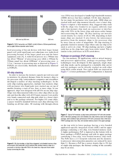
vias (TSVs) was developed to handle high-bandwidth memory
                                                             (HBM) devices that have multiple 128-bit data channels—
                                                             far too many for perimeter wire bond pads. HBM chips are
                                                             stacked with each chip mounted directly over a lower chip.
                                                             Figure 6 depicts a four-memory chip, staggered-chip stack
                                                             with the chips wire bonded to an organic substrate (top)
                                                             and a four-memory chip stack on a processor or interface
                                                             chip with TSVs in the lower chips and micro-solder bumps
                                                             interconnecting the chips. 3D chip stacking can increase
                                                             circuit density by a factor of 2X to 10X, depending on how
                                                             many chips are stacked. It also lowers the interconnect
                                                             parasitics from the memory chips to the processor chip
                                                             by more than an order of magnitude. 3D chip stacking is
        Figure 5: FOPLP versus fan-out FOWLP: a) (left) 450mm x 550mm panel format;   generally limited to memory chips where only one chip in the
        and b) (right) 300mm diameter wafer format.          stack is active at a time. 3D chip stacking can have a higher
        level processing of fan-out devices with their larger format   yield loss as the chips have only been wafer tested. This is
        panels will yield significant cost reductions over wafer-level   similar to the yield issues in ECPs noted above.
        processing because of the larger panel area and the lower
        equipment costs [4]. A wafer-level process on a 300mm line   Package-on-package (PoP) stacking
                        2
        has about 70Kmm  of processing area while a 450mm by   For non-memory 3D applications such as mixed memory
                                      2
        550mm panel has about 240Kmm  of processing area—a   and  processor  applications,  package-on-package  (PoP)
        3.5 to 1 increase in processing area as depicted in Figure 5.   technologies were developed. In this approach, single chips
        FOPLPs are electrically, thermally and physically identical   and chip stacks can be packaged in a stackable chip carrier
        to FOWLPs.                                           and two packages can be directly stacked on each other
                                                             using BGA solder attach. Two typical PoPs are depicted in
        3D-chip stacking                                     Figure 7. A lower performance PoP configuration is depicted
          In order to increase the memory capacity per unit area and
        to minimize the physical distance from the memory chips to
        the processor chip, semiconductor companies and assemblers
        developed a number of chip stacking technologies. In the
        early chip stacking approaches, multiple bare memory chips
        with perimeter wire bond pads were stacked one on top of
        another forming a stack of two, four, or more chips. In one
        approach, chips were designed with all I/Os on one chip edge.
        Chips were then mounted with every other chip offset on one
        side and then the other with all I/O pads exposed. Low-profile
        wire bonds connected each chip pad either to a lower chip’s
        pad or to the package substrate. For higher I/O count chips,
        a spacer would be mounted between each chip allowing wire
        bonding on all four sides. 3D stacking with through-silicon


                                                             Figure 7: Typical PoP modules: a) (top) lower performance PoP with wire bonded
                                                             ASIC in the lower package and a wire bonded, two-chip memory stack on the upper
                                                             package; and b) (bottom) high-performance PoP with a processor chip in the lower
                                                             FOPLP package and a four-chip, wire bonded memory stack in the upper package.
                                                             on the top with its lower package having a wire bonded
                                                             application-specific integrated circuit (ASIC) and its upper
                                                             package containing a two-chip, wire-bonded memory stack.
                                                             A higher performance PoP is depicted on the bottom with its
                                                             lower package a FOPLP package and with its upper package
                                                             containing a four-chip, wire-bonded memory chip stack.
                                                             The PoPs have a 2:1 footprint reduction and the memory-
                                                             to-processor interconnection parasitics are reduced by more
        Figure 6: 3D chip stacking: a) (top) three staggered, wire bonded memory chips   than 2:1. Because a PoP has a power density that is 2X that
        on an organic BGA substrate; and b) (bottom) four stacked memory chips on a   of single-chip packages, the thermal cooling of the assembly
        processor or interface chip with TSVs in the lower four chips and micro-solder   may be an issue.
        bumps connecting the chips.

                                                                                                             13
                                                       Chip Scale Review   November  •  December  •  2021   [ChipScaleReview.com]  13