
Page 14 - Chip Scale Review_November December_2021-digital
P. 14
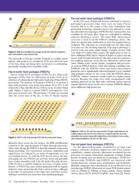
Fan-out wafer-level packages (FOWLPs)
                                                               As the I/O count of high-end devices continued to increase,
                                                             particularly processor chips, there were too many I/Os to
                                                             reliably fan in to the center of the chip. Embedded chip
                                                             packaging technology (detailed above) was utilized to create
                                                             fan-out wafer-level packages (FOWLPs) that increased the area
                                                             available for I/O pads. Bare chips are embedded in molding
                                                             material forming a carrier. The same RDL interconnect
                                                             structure is used as on the FIWLP technology above. The
                                                             chips are spaced apart sufficiently to form the required device
                                                             footprint. The chip pads are routed both over the chip center
                                                             area and over the molding material. Flip-chip technology is
                                                             used to form area array solder bumps. Complex devices with
        Figure 2: Multi-chip embedded chip package: a) (top) Five-chip ECP, perspective   very high I/O counts often require the application of one or
        view; and b) (bottom) cross-sectional view.          more additional RDL layers. Figure 4 depicts a typical fan-out
        The downside of having a smaller footprint is a higher power   device with I/O pads formed over the chip center area and over
        density  that needs to be considered. ECPs also have the issue   the molding material. Early fan-out fabricators utilized the
        of the bare chips not being fully tested prior to embedding,   same 300mm wafer carrier format, equipment and processes
        potentially causing lower assembly yields.           as used on FIWLP devices, while also adding a molding step.
                                                             FOWLPs like the FIWLPs above had lower interconnect
        Fan-in wafer-level packages (FIWLPs)                 parasitics, and a significantly reduced footprint versus standard
          Fan-in wafer-level packages (FIWLPs) are chip-scale   chip packages (about 4:1 less area). Like the FIWLPs above,
        packages (CSPs) that are fabricated at wafer level as an   FOWLPs’ smaller footprint would result in a higher power
        extension of semiconductor fabrication back-end-of-line (BEOL)   density. Because the chips were fully encapsulated, with
        processing. The purpose of forming a FIWLP is to convert a   molding material on the chip sides and back surface and an
        chip with perimeter wire bond pads (about 90 to 95% of all   organic dielectric layer on the active surface, FOWLPs offered
        chips) into a flip-chip like device with an array of solder bump   some additional chip protection.
        pads. Figure 3 depicts a typical FIWLP in perspective view
        and cross-sectional view. The perimeter I/O pads are rerouted
        onto the center area of the die. A thin (5–10µm) organic


                                                             Figure 4: FOWLP or PLP with the chip perimeter I/O pads routed both over the
                                                             molding material and over the chip center area. a) (top) Perspective view with
                                                             embedded chip position shown with dashed lines; and b) (bottom) Cross-section
        Figure 3: FIWLP or chip-scale package (CSP) with area array solder bumps.
                                                             view showing embedded chip with two RDL layers.
        dielectric layer covers the die surface. An RDL metallization
        connects to the chip perimeter I/O pads through microvias.   Fan-out panel-level packages (FOPLPs)
        After wafer dicing, the FIWLP is then flip attached using solder   As  the  photolithography  capabilities  of  high-end
        bump technology. The interconnect resistance, inductance and   organic substrate facilities improved with finer feature
        capacitance are reduced by an order of magnitude over the   capabilities, organic substrate fabricators developed fan-out
        wire bonded device. As with the ECP devices above, the bare   processes on organic fabrication equipment in larger format
        chip going into the FIWLPs are not fully tested and generally   panels forming fan-out panel-level packages (FOPLPs).
        have a lower assembly yield. Like the earlier flip-chip devices,   Structurally, FOWLPs and FOPLPs are identical with
        FIWLPs have a smaller footprint and have a higher power   similar materials, feature sizes, performance and footprints.
        density. A FIWLP has some surface protection with its organic   Multiple companies have introduced, or are in the process of
        dielectric layer protecting the chip’s active surface, although   introducing, FOPLPs fabricated on larger PCB format panels
        it provides no protection to the chip sides and back surface   such as 450mm by 550mm or larger panels. These include
        making it somewhat less protective than standard packages.  Amkor, Deca, SPTS, STATS ChipPAC, and others [3]. Panel-


        12
        12   Chip Scale Review   November  •  December  •  2021   [ChipScaleReview.com]