Page 20 - Chip Scale Review_November December_2021-digital
P. 20
A new, higher density QFP


        By Chu-Chung (Stephen) Lee, Yao Jinzhong, Glenn G. Daves  [NXP Semiconductors N.V.]
        This technical article (part 2) is a continuation of the Emerging Technologies column entitled, “A new, higher density QFP”
        in the September • October 2021 issue of Chip Scale Review.
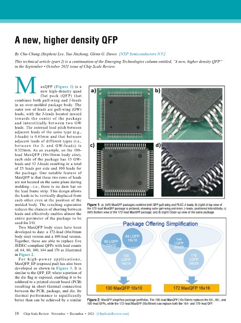
        M            axQFP (Figure 1) is a


                     new high-density quad
                     f lat pack (QFP) that
        combines both gull-wing and J-leads
        in an over-molded package body. The
        outer row of leads are gull-wing (GW)
        leads, with the J-leads located inward
        towards the center of the  package
        and interstitially between two GW
        leads. The external lead pitch between
        adjacent leads of the same type (e.g.,
        J-leads) is 0.65mm and that between
        adjacent leads of different types (i.e.,
        bet ween the J- and GW-leads) is
        0.325mm. As an example, on the 100-
        lead MaxQFP (10x10mm body size),
        each side of the package has 13 GW-
        leads and 12 J-leads resulting in a total
        of 25 leads per side and 100 leads for
        the package. One notable feature of
        MaxQFP is that these two rows of leads
        are not located on the same plane during
        molding—i.e., there is no dam bar on
        the lead frame strip. This design allows
        the leads to be vertically displaced from
        each other even at the position of the
        molded body. The resulting separation   Figure 1: a): (left) MaxQFP packages combine both QFP gull-wing and PLCC J-leads; b) (right) A top view of
        reduces the chances of shorting between   the 172-lead MaxQFP package is pictured, showing outer gull-wing and inner J-leads, positioned interstitially; c)
        leads and effectively enables almost the   (left) Bottom view of the 172-lead MaxQFP package; and d) (right) Close-up view of the same package.
        entire perimeter of the package to be
        used for I/O.
          Two MaxQFP body sizes have been
        developed to date: a 172-lead (16x16mm
        body size) version and a 100-lead version.
        Together, these are able to replace five
        JEDEC-compliant QFPs with lead counts
        of: 64, 80, 100, 144 and 176 as illustrated
        in Figure 2.
          Fo r  h ig h - p owe r  a p pl ic a t io n s ,
        MaxQFP_EP (exposed pad) has also been
        developed as shown in Figure 3. It is
        similar to the QFP_EP, where a portion of
        the die flag is exposed, enabling it to be
        soldered to a printed circuit board (PCB)
        resulting in short thermal connection
        between the PCB, package, and die. Its
        thermal performance is significantly
        better than can be achieved by a similar   Figure 2: MaxQFP simplifies package portfolios. The 100-lead MaxQFP (10x10mm) replaces the 64-, 80-, and
                                           100-lead QFPs, while the 172-lead MaxQFP (16x16mm) can replace both the 144- and 176-lead QFP.

        18   Chip Scale Review   November  •  December  •  2021   [ChipScaleReview.com]
        18

