Page 29 - Chip Scale Review_November December_2021-digital
P. 29
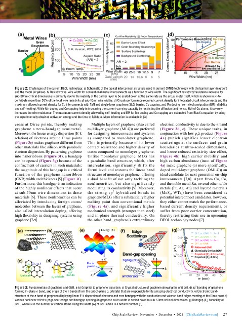
Figure 2: Challenges of the current BEOL technology: a) Schematic of the typical interconnect structure used in current CMOS technology with the barrier layer (in green)
        and the metal (in yellow). b) Resistivity vs. wire width for conventional metal interconnects as a function of wire width. The significant resistivity/resistance increase for
        sub-20nm critical dimensions is primarily due to the inability of the barrier layer to be scaled down at the same rate as the actual metal itself, which is shown in (c) to
        contribute more than 50% of the total wire resistivity at sub-10nm wire widths. d) Circuit-performance required current density for integrated circuit interconnects and the
        maximum allowed current density for Cu interconnects with TaN and single-layer graphene (SLG) barrier, Co capping, and Mn doping (from electromigration (EM) reliability
        and self-heating). While Mn doping and Co capping help in increasing the current-carrying capacity by restricting the diffusion (and hence, EM) of Cu atoms, it severely
        increases the wire resistance. The maximum current density allowed by self-heating and EM for Mn doping and Co capping are estimated from Black’s equation by using
        the experimentally obtained activation energy and the time to fail data. More information is available in [3].
        cross at Dirac points, thereby making   Multiple layers of graphene (also called   electrical conductivity is due to the π band
        graphene a zero-bandgap semimetal.   multilayer graphene (MLG)) are preferred   (Figure 3d, e). These unique traits, in
        Moreover, the linear energy dispersion (E-k   for designing interconnects and systems   conjunction with low ρ 0 λ product (Figure
        relation) of electrons around Dirac points   as compared to monolayer graphene.   4a) (which signifies lesser electron
        (Figure 3e) makes graphene different from   This is primarily because of its lower   scatterings at the surfaces and grain
        other materials like silicon with parabolic   contact resistance and higher density of   boundaries at ultra-scaled dimensions,
        electron dispersion. By patterning graphene   states compared to monolayer graphene.   and hence reduced resistivity size effect,
        into nanoribbons (Figure 3f), a bandgap   Unlike monolayer graphene, MLG has   Figure 4b), high carrier mobility, and
        can be opened (Figure 3g) because of the   a parabolic band structure, which, after   high carbon abundance (inset of Figure
        confinement of carriers in such materials;   intercalation, significantly shifts the   4a) make graphene (or more specifically,
        the magnitude of this bandgap is a critical   Fermi level and restores the linear band   doped multi-layer graphene (DMLG)) an
        function of the graphene nanoribbon   structure of monolayer graphene, offering   ideal candidate for next-generation on-chip
        (GNR) width and thickness [5] (Figure 3f).   a dual benefit of not only tackling the   interconnects [7,8]. Apart from Cu, Co,
        Furthermore, this bandgap is an indication   nonlinearities, but also significantly   and the noble metal Ru, several other noble
        of the highly nonlinear effects that occur   modulating its conductivity [9]. Moreover,   metals (Pt, Ag, Au) and layered materials
                                                        2
        at sub-50nm wire dimensions in these   the strong sp  hybridized bonds in   (MoS 2 , WTe 2 ) have been considered as
        materials [6]. These nonlinearities can be   graphene/MLG offer a substantially higher   potential interconnect candidates, however,
        alleviated by introducing foreign atoms/  melting point than conventional metals   they either cannot match the performance-
        molecules between the layers of graphene,   (Figure 4a), and significantly higher   based current density requirements, or
        also called intercalation doping, offering   mechanical strength (stronger than steel)   suffer from poor carrier concentration,
        high flexibility in designing systems using   and in-plane thermal conductivity. On   thereby restricting their use in upcoming
        graphene [7-9].                    the other hand, graphene’s extraordinary   BEOL technology nodes [7].


                                                                                                2
        Figure 3: Fundamentals of graphene and GNR. a-b) Graphite to graphene transition; c) Crystal structure of graphene showing the unit cell. d) sp  bonding of graphene
        forming in-plane σ band, and origin of the π bands (from the out-of-plane p z  orbitals) that are responsible for its amazing electrical conductivity. e) Electronic band-
        structure of the π band of graphene displaying linear E-k dispersion of electrons and zero bandgap with the conduction and valence band edges meeting at the Dirac point. f)
        Various nonlinear effects (edge scatterings and bandgap opening) in graphene as its width is scaled down to sub-50nm critical dimensions. g) Bandgap (E g ) tunability of
        GNR, where N is the number of carbon atoms along the width (w) of GNR and n is a natural number [5].

                                                                                                             27
                                                       Chip Scale Review   November  •  December  •  2021   [ChipScaleReview.com]  27

