Page 30 - Chip Scale Review_November December_2021-digital
P. 30
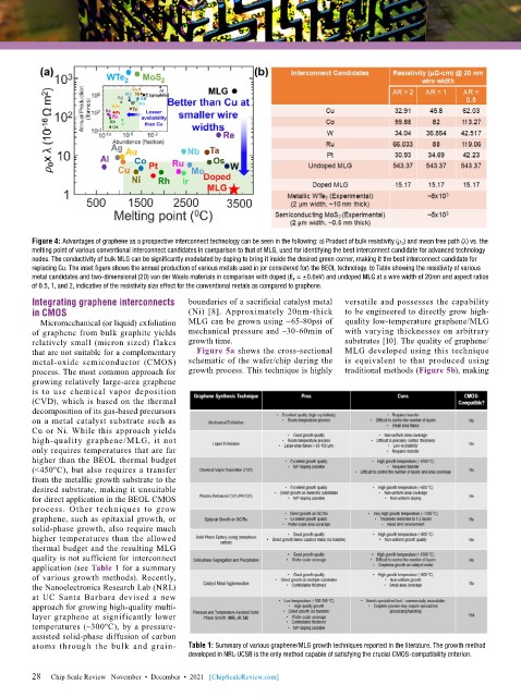
Figure 4: Advantages of graphene as a prospective interconnect technology can be seen in the following: a) Product of bulk resistivity (ρ 0 ) and mean free path (λ) vs. the
        melting point of various conventional interconnect candidates in comparison to that of MLG, used for identifying the best interconnect candidate for advanced technology
        nodes. The conductivity of bulk MLG can be significantly modulated by doping to bring it inside the desired green corner, making it the best interconnect candidate for
        replacing Cu. The inset figure shows the annual production of various metals used in (or considered for) the BEOL technology. b) Table showing the resistivity of various
        metal candidates and two-dimensional (2D) van der Waals materials in comparison with doped (E F  = ±0.6eV) and undoped MLG at a wire width of 20nm and aspect ratios
        of 0.5, 1, and 2, indicative of the resistivity size effect for the conventional metals as compared to graphene.
        Integrating graphene interconnects   boundaries of a sacrificial catalyst metal   versatile and possesses the capability
        in CMOS                            (Ni) [8]. Approximately 20nm-thick   to be engineered to directly grow high-
          Micromechanical (or liquid) exfoliation   MLG can be grown using ~65-80psi of   quality low-temperature graphene/MLG
        of graphene from bulk graphite yields   mechanical pressure and ~30-60min of   with varying thicknesses on arbitrary
        relatively small (micron sized) flakes   growth time.                 substrates [10]. The quality of graphene/
        that are not suitable for a complementary   Figure 5a shows the cross-sectional   MLG developed using this technique
        metal-oxide semiconductor (CMOS)   schematic of the wafer/chip during the   is equivalent to that produced using
        process. The most common approach for   growth process. This technique is highly   traditional methods (Figure 5b), making
        growing relatively large-area graphene
        is to use chemical vapor deposition
        (CVD), which is based on the thermal
        decomposition of its gas-based precursors
        on a metal catalyst substrate such as
        Cu or Ni. While this approach yields
        high-quality graphene/MLG, it not
        only requires temperatures that are far
        higher than the BEOL thermal budget
        (<450ºC), but also requires a transfer
        from the metallic growth substrate to the
        desired substrate, making it unsuitable
        for direct application in the BEOL CMOS
        process. Other techniques to grow
        graphene, such as epitaxial growth, or
        solid-phase growth, also require much
        higher temperatures than the allowed
        thermal budget and the resulting MLG
        quality is not sufficient for interconnect
        application (see Table 1 for a summary
        of various growth methods). Recently,
        the Nanoelectronics Research Lab (NRL)
        at UC Santa Barbara devised a new
        approach for growing high-quality multi-
        layer graphene at significantly lower
        temperatures (~300ºC), by a pressure-
        assisted solid-phase diffusion of carbon
        atoms through the bulk and grain-  Table 1: Summary of various graphene/MLG growth techniques reported in the literature. The growth method
                                           developed in NRL-UCSB is the only method capable of satisfying the crucial CMOS-compatibility criterion.

        28   Chip Scale Review   November  •  December  •  2021   [ChipScaleReview.com]
        28

