Page 34 - Chip Scale Review_November December_2021-digital
P. 34
Figure 7: Graphene interconnect technology development timeline at NRL, UCSB: Evolution of graphene as an interconnect technology from the first proposal of doped
        graphene interconnects in 2008 to the demonstration of CMOS-compatible multi-level graphene interconnects in 2020.
        interconnects is being actively evaluated,   grow high-quality MLG on 300mm   of inductors has remained basically
        and has been demonstrated to reduce   industry standard wafers, making    unchanged since their invention almost
        overall resistance by 15%  [15]. With that   this technique extremely versatile and   two  centuries  ago.  NRL  at  UCSB
        in mind, NRL recently demonstrated   industry friendly.               overcame this fundamental scaling
        BEOL-compatible growth of high-                                       challenge by evoking sizable “kinetic
        quality MLG directly on Cu by inserting   Intercalated MLG inductors   inductance (K I)” (Figure 9b) in
        ~2nm amorphous carbon layer between   overcome a 200-year-old limit   intercalation-doped MLG inductors
        Ni and Cu [10]. In principle, with a smart   On-chip  inductors  are  essential   at room temperat u re, leadi ng to
        choice of the overall growth conditions,   components in almost all modern   materials with the highest inductance
        and a thorough knowledge of the relative   electronic gadgets such as smartphones   densities ever created [9]. In contrast
        diffusion coefficients of carbon in the   and computers and can occupy up to   to conventional magnetic inductance,
        growth catalyst and growth substrate,   50% of the total chip area. However,   kinetic  inductance  arises  from  the
        this technique can be engineered to grow   unlike all other IC components that   intrinsic inertia of the charge carriers
        MLG on various metallic (Co, Ru, W, Pt,   shrink with each technology node,   and appears in series with magnetic
        etc.) and dielectric surface topologies.   inductors are hard to scale down as they   inductance, hence increasing the
        Moreover, the current wafer coverage   solely rely on their magnetic inductance   overall inductance for a given inductor
                 2
        of ~10mm  can be expanded to directly   (Figure 9a). Therefore, the design   footprint (Figure 9b). Intercalation


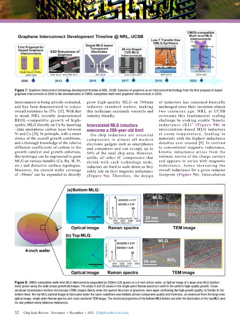
        Figure 8: CMOS-compatible multi-level MLG interconnects (separated by 200nm ILD) grown on a 4-inch silicon wafer. a) Optical image of a large-area MLG (bottom
        level) grown using the solid-phase growth technique. The sharp G and 2D peaks in the single-point Raman spectrum confirm the uniform high-quality growth. Cross-
        sectional transmission electron microscope (TEM) images clearly show the layered structure of graphene, once again confirming the high growth quality. b) Similar to the
        bottom-level, the top MLG (optical image) is fabricated under the same conditions and exhibits almost comparable quality and thickness, as evidenced from the large area
        optical image, single-point Raman spectra and cross-sectional TEM image. The electrical properties of the bottom MLG before and after the fabrication of the top MLG (and
        Co-via) yielded nearly identical resistances.

        32
        32   Chip Scale Review   November  •  December  •  2021   [ChipScaleReview.com]

